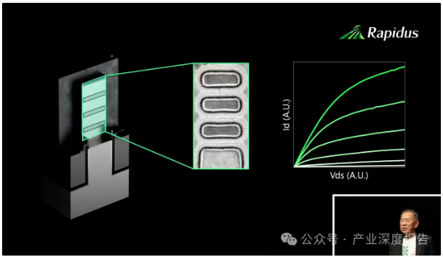
On August 27, news emerged from the recently concluded Hot Chips 2025 conference that the Japanese semiconductor company Rapidus announced the successful completion of 2nm GAA (Gate-All-Around) test chip tape-out (note: the actual tape-out was successfully completed on July 10), with plans for mass production in 2027.

The 2nm chip is based on ASML extreme ultraviolet (EUV) lithography, and the node process has met all preset electrical performance indicators. In 2027, Rapidus expects to achieve a monthly capacity of 25,000 wafers at its IIM-1 factory.
Additionally, Rapidus also introduced at the Hot Chips conference the development goals of the IIM-1 factory and its appeal to potential customers. Compared to TSMC and possibly Intel, Rapidus will lag behind in process technology by one to two nodes in 2027. The company aims to achieve differentiation through production flexibility:
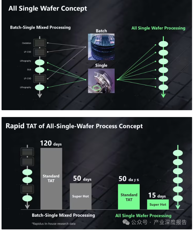
Single wafer process concept: The cycle from design to wafer completion can be shortened to 50 days, while traditional batch– single wafer hybrid processes typically take about 120 days.
Rapid delivery: To meet urgent demands for specific products, the standard delivery cycle is 50 days, Rapidus commits to achieving 15 days wafer delivery at the 2nm node, which is unprecedented in the industry.
Rapidus stated that this model relies on customized backend processes, combined with OSAT, EDA, IP, R&D, and material supply chains to achieve rapid tape-out and delivery.
In less than three years, Rapidus has completed major milestones for the IIM-1 factory: Groundbreaking in September 2023, installation and connection of over 200 advanced semiconductor equipment in June 2025.
Rapidus’s execution capability will be a key indicator. Currently, the company’s vision has a certain degree of credibility, but the semiconductor manufacturing industry is complex and ever-changing, and many plans may not be fully realized on schedule, so the outside world is still closely monitoring its progress.