Currently, using Keil C51 and Proteus for microcontroller system development has become the first choice for many microcontroller enthusiasts. The combination of Keil C51 and Proteus allows for software design and hardware simulation debugging of microcontroller systems, which can greatly shorten the development cycle and reduce development and debugging costs. Once the simulation debugging is successful, we can use Proteus 6 Professional and ARES 6 Professional for PCB design and production. Many articles or books discuss how to use Keil C51 + Proteus for the design and simulation development of microcontroller application systems, but there are few mentions of using Proteus to create printed circuit boards (PCBs). This article takes a simple advertisement light design circuit (as shown in Figure 1) as an example to discuss how to use Proteus to create PCBs.
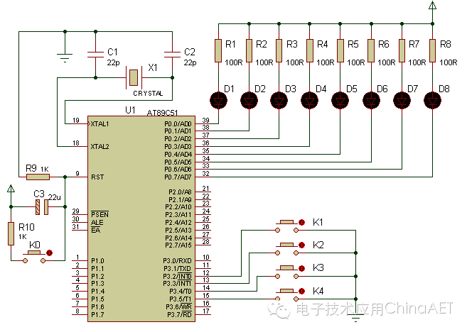
Figure 1 Design circuit of the advertisement light
Using Proteus to create PCBs typically includes the following steps: (1) draw the circuit schematic and simulate debugging; (2) load the netlist and component packages; (3) plan the circuit board and set relevant parameters; (4) component layout and adjustment; (5) wiring and adjustments; (6) output and production of PCB.
1. Draw the circuit schematic and simulate debugging
In Proteus 6 Professional, design the circuit schematic using ISIS 6 Professional, and combine it with Keil C51 for software programming and hardware simulation debugging. Once debugging is successful, you can start making the PCB. The debugging process will not be elaborated here.
2. Load the netlist and component packages
(1) Load the netlist
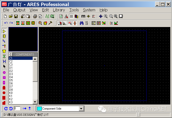
Figure 2 ARES 6 Professional window
In the ISIS 6 Professional interface, click the  icon in the Design Toolbar or open the ARES 6 Professional window through the Netlist to ARES command in the Tools menu, as shown in Figure 2. In the lower left corner of Figure 2, you can see the component selection window, which lists all the components loaded from the schematic. If some components in the schematic do not automatically load the package or if there is no suitable package in the package library, a dialog box will pop up requesting the selection of a package when loading the netlist, as shown in Figure 3. At this point, you need to manually select and load according to the specific components and their packages.
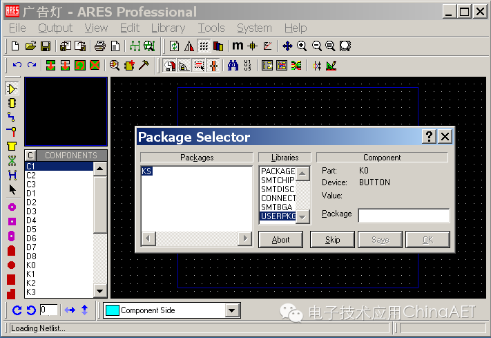
Figure 3 Dialog box requesting package selection
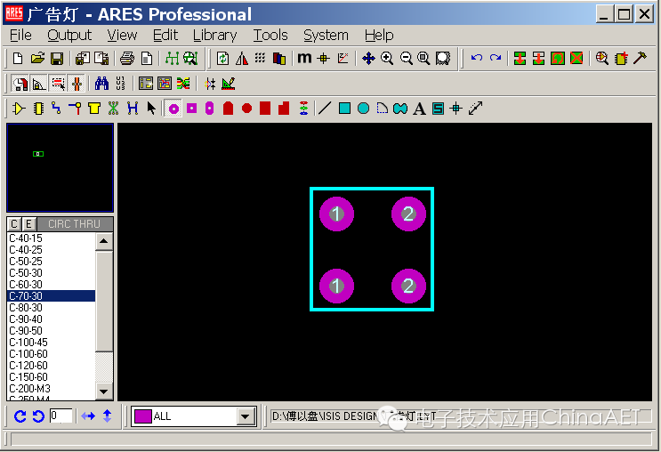
Figure 4 Completed button package design
(2) Design component packages
If the package is not available in the package library or does not match the actual component, you need to create it yourself. So, how do you draw the package? Here, we take the button switch in the example as an example to design a component package.
1. Place pads
In the interface shown in Figure 2, place 4 pads according to the pin spacing of the button, and modify the pad numbers to match the component pin numbers in the schematic; otherwise, an error message will pop up indicating no network connection, or there will be no connections after loading.
2. Place the outer frame
Use the  icon in the 2D drawing tools to add an outer frame based on the actual size of the button, thus completing the button package design (as shown in Figure 4).
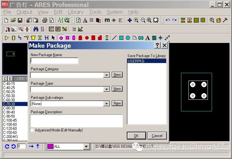
Figure 5 Save package dialog box
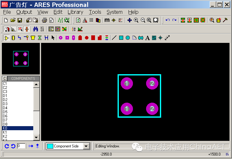
Figure 6 Load package dialog box
3. Save the package
Select the package, left-click the  icon, and the save dialog box will appear (as shown in Figure 5). Enter the name of the component package to be saved (here using KS) in New Package Name; select Miscellaneous in Package Category; select Through Hole in Package Type; select Switches in Package Sub-Category; click OK, and the button package will be saved in the USERPKG (user-defined package library).
4. Load the package
After saving the self-built package, go to the library to load it, and you can load the component package you created into the PCB (as shown in Figure 6).
After drawing all the required component packages using the above method, click the  icon in the Design Toolbar from the schematic to reload the netlist, thus loading all components into the PCB.
3. Plan the circuit board and set relevant parameters
(1) Plan the circuit board
In the ARES 6 Professional window, select the  icon in the 2D drawing toolbar, and select the Board Edge layer (yellow) in the bottom circuit layer to click and drag to draw the PCB board’s border. The size of the border is the size of the PCB, so when drawing the border, it should be based on the actual measurements using the measuring tool
  (as shown in Figure 7).
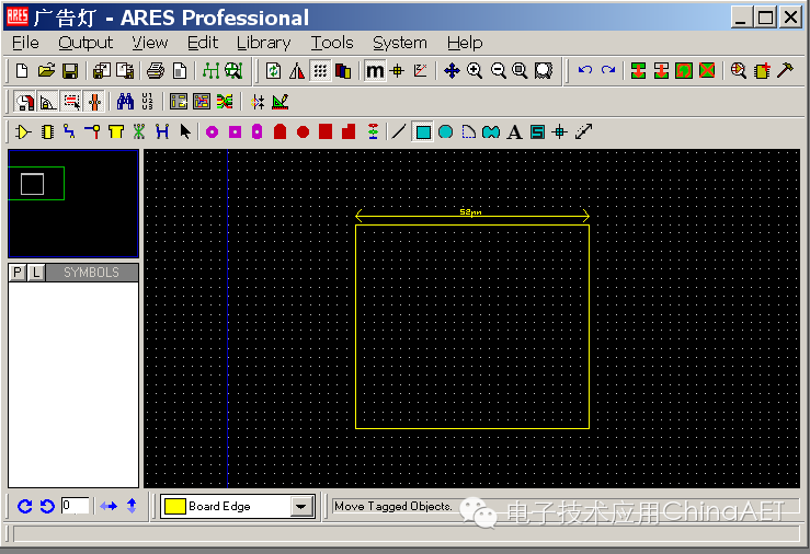
Figure 7 Circuit board planning diagram
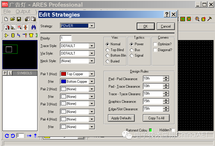
Figure 8 Setting related parameters of the circuit board
(2) Set the relevant parameters of the circuit board
Once the PCB board border is drawn, set the relevant parameters of the circuit board. Click on Set Default Rules in the System, and set the rule parameters in the pop-up dialog box, including pad spacing, line to pad spacing, line to line spacing, and other safety allowable values. Then select the  (routing rules) option in Tools, and click Edit Strategies in the pop-up dialog box, which appears as shown in Figure 8. In the left upper Strategy column, select POWER and SIGNAL, and in the Pair1 below, select the same layer. This completes the wiring settings for a single-layer board. At this point, the main parameter settings are complete. Other system parameter settings can be completed in System and Tools.
4. Component layout and adjustment
(1) Component layout
Once the circuit board rules are designed, components can be imported and laid out. There are two ways for layout: automatic layout and manual layout. If using the automatic layout method, simply select the  option in the menu bar, and a dialog box will pop up. Click OK, and the components will be automatically laid out on the PCB. If using the manual layout method, select the components from the component selection window in the lower left corner and left-click at an appropriate position on the PCB board border to place the component.
(2) Component adjustment
Whether using automatic or manual layout, components need to be adjusted. This mainly involves moving and flipping the components. The layout principle for components is: aesthetics, ease of wiring, and making the PCB as small as possible. The component layout of the PCB is completed as shown in Figure 9.
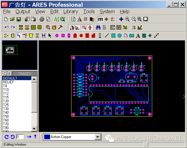
Figure 9 Completed component layout of the PCB
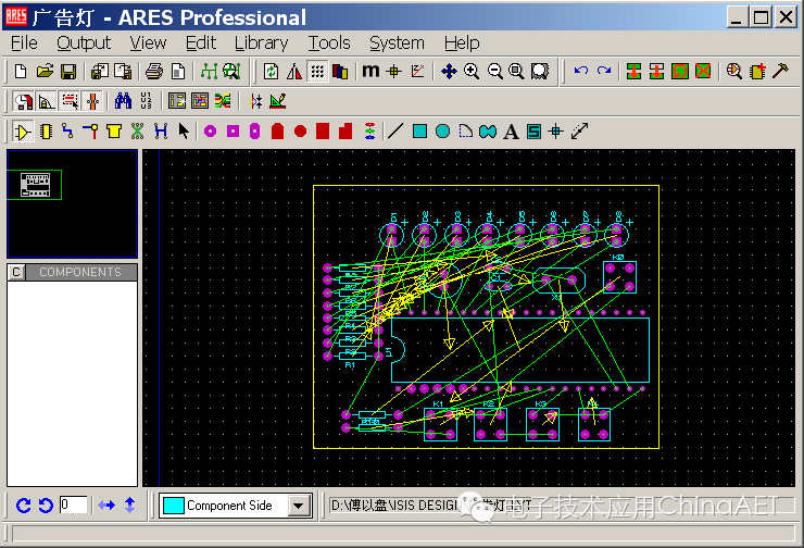
Figure 10 Completed wiring diagram
5. Wiring and adjustments
Similarly, PCB wiring can be done using either automatic or manual wiring methods. Generally, automatic wiring is done first, followed by manual modification, or you can directly do manual wiring. The wiring rules have been described above; here we mainly explain the thickness settings of the wires used for wiring and the modification of pad sizes. First, select the  option in the tool menu bar, select the desired wire thickness type in the wire selection window in the lower left corner, or choose DEFAULT (default), then click the E button to modify the Width value in the pop-up dialog box. During the wiring process, if you need to change the size of a particular wire, you can right-click to select the appropriate type in the Trace Style option; to delete the wire, left-click Delete. If you want to delete the entire wiring, select all connections and left-click the
  icon in the tool menu bar. Modifications to pads can be made after wiring is complete. First, select the
  option in the tool menu bar, then select the appropriate pad in the selection window, and left-click at the pad of the component that needs to be changed. The completed PCB after wiring is shown in Figure 10. (Note: 1000th = 1 inch = 25.4 mm)
6. Output and production of PCB
Finally, output the printed circuit layout. First, click on Set Output Area in the Output option, hold down the left mouse button, and drag to select the layout to be output, as shown in Figure 11.
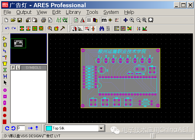
Figure 11 Output printing circuit layout
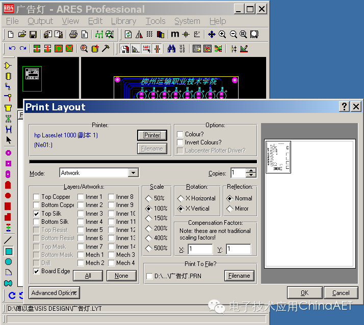
Figure 12 Setting the output circuit layer to print
Next, set the output circuit layer to print. In the Output option, click on Print/Plot Layout, and a settings dialog box will appear, as shown in Figure 12.
In the settings dialog box, click to select Printer, where you can choose the printer and set the printing paper size and layout placement direction. In the Layers/Artworks section below, select the layers to be printed. Since wiring is done on the bottom layer, when printing the wiring layer, check the Bottom Copper and Board Edge options to indicate the layers to be printed; when printing the component layout layer (silkscreen layer), check the Top Silk and Board Edge options (note that this layer needs to be selected for mirrored printing during printing); the Scale option is the scale of the printed output, set to 100%; Rotation and Reflection options are for horizontal/vertical output and whether to mirror the settings. Once set, printing can proceed, as shown in Figures 13 and 14, which are the printing effects of the silkscreen layer and the wiring layer, respectively.
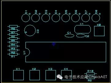
Figure 13 Printing effect of the silkscreen layer
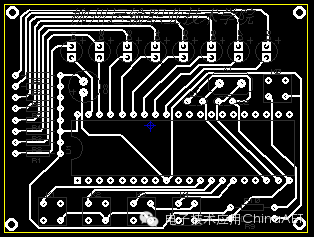
Figure 14 Printing effect of the wiring layer
Thus, we have completed the entire process of using Proteus to create printed circuit boards.