ClickBlueTextFollow Us01Overview of MUX
A multiplexer (MUX) is a classic combinational logic unit in digital circuit design. It has multiple input signals and a single output port, with its core function being to select one specified input signal as output based on external selection signals. MUX plays a critical role in communication systems, data processing paths, and various programmable logic devices, serving as a fundamental component for signal routing and data distribution.
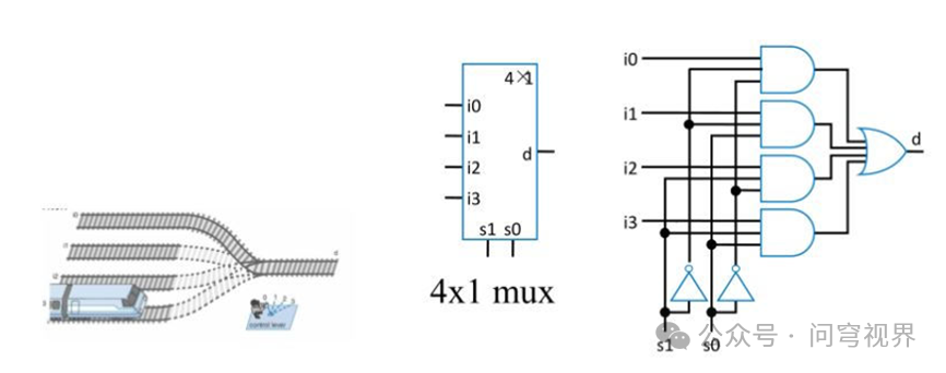 02MUX in FPGA
In the structure of an FPGA, MUX is embedded as a basic logic element within configurable logic blocks (CLBs). By examining the internal structure diagram of FPGA devices and zooming in, one can clearly identify MUX units specifically designed to implement multiplexing functions, typically laid out in a specific logic block form between routing resources.
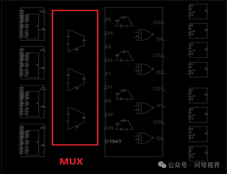
The red part marked in the image indicates the MUX, showing that MUX exists as a basic component within the FPGA.
A question worth exploring is: since MUX, as a combinational logic circuit, can be fully implemented by lookup tables (LUTs), why are dedicated MUX hardware resources additionally designed in FPGA architectures?
In fact, for smaller selectors, such as two-to-one (MUX2), three-to-one (MUX3), or four-to-one (MUX4), FPGAs generally use LUTs for implementation. For example, each six-input LUT (LUT6) can be configured as a four-to-one MUX. Next, we will take MUX4 as an example to see how FPGA implements MUX using LUT.
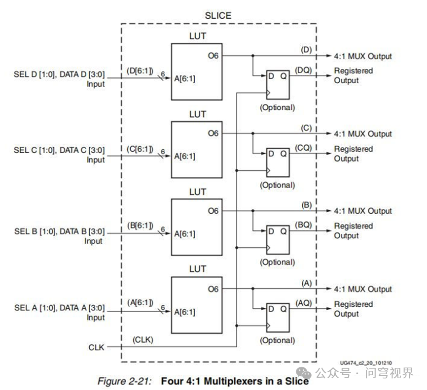
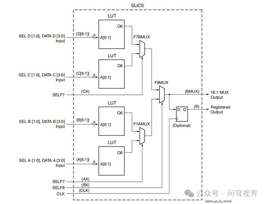
The specific implementation method is to map two address selection signals and four data input signals to the input ports of the LUT, achieving data selection functionality through pre-stored truth tables. Therefore, up to four MUX4 units can be configured within a single Slice.
However, when the required number of input lines exceeds four, the number of input ports of a single LUT6 is insufficient to support it. At this point, the dedicated MUX resources in the FPGA come into play. For example, an eight-to-one MUX (MUX8) typically combines LUTs with F7AMUX and F7BMUX located within the same Slice. These two dedicated MUX units can combine the outputs of two LUTs to construct a combinational logic function supporting up to thirteen inputs (or a single 8:1 MUX). A maximum of two MUX8 structures can be implemented within a single Slice.
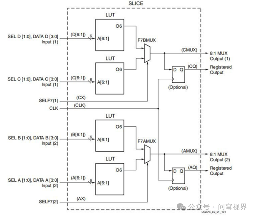
Furthermore, if a sixteen-to-one MUX (MUX16) needs to be implemented, the F8MUX in the Slice can use the outputs of F7AMUX and F7BMUX as its inputs, forming a combinational logic that supports up to twenty-seven inputs (or a single 16:1 MUX). Typically, only one MUX16 structure can be deployed in each Slice.
Although larger MUX can theoretically be constructed using multiple SLICEM modules, the lack of dedicated fast interconnect resources between Slices limits implementation efficiency and timing performance.
This design approach, based on LUTs supplemented by hierarchical dedicated MUX, not only expands the implementation scale of MUX but also ensures that the overall logic structure possesses good symmetry. Symmetrical layout helps to make signal routing delays between modules more consistent, thereby reducing timing deviations and enhancing system stability.
 03Conclusion
From the above analysis, it can be seen that when implementing MUX functionality in FPGA, both the flexible configuration of LUTs and the dedicated MUX units in the chip can be utilized. This raises a thought-provoking question: since LUT can achieve all the functions of MUX, why not completely replace dedicated MUX with it? For example, when implementing an MUX8, besides using the “two LUTs + one dedicated MUX” scheme, it could theoretically also use a combination of “three LUTs”.
In reality, retaining dedicated MUX in FPGA is a rational choice made after various considerations, primarily based on the following factors:
First is the cost factor. MUX is used very frequently in digital systems, and dedicated MUX, as a logic unit with fewer transistors, typically saves more hardware resources than LUT structures based on storage units when implementing the same function. LUTs rely on storage units to hold logical functions, and the number of transistors consumed by their control and connection structures is significantly higher. Therefore, using dedicated MUX can greatly reduce implementation costs while ensuring functionality.
Additionally, if all multiplexing functions were implemented using LUTs, it would not only waste logical resources but could also negatively impact timing performance and power consumption due to increased routing complexity. Dedicated MUX has clear advantages in path delay and area efficiency, especially suitable for high-frequency and high-fan-out scenarios.
Thus, the design that integrates LUTs and dedicated MUX in FPGA architecture is essentially a precise balance achieved between flexibility, cost, and performance.
Understanding the implementation principles of MUX in FPGA not only deepens the understanding of hardware architecture but also directly guides engineering practice. For instance, when HDL code (such as case statements) is synthesized into wide MUX, designers should be aware that it is likely mapped to the dedicated MUX chain within the Slice, which usually indicates better timing characteristics. Clearly describing selection logic helps synthesis tools accurately identify MUX structures and map them to optimal hardware resources, thereby avoiding redundant logic. At the same time, understanding the fixed layout of these dedicated resources also helps explain why synthesis tools often tightly “pack” related logic within a few Slices—this is precisely to utilize the internal high-speed paths, further enhancing system performance.