The bathroom is a place we visit every day. Turning the light on and off when entering and exiting can be quite a hassle. Sometimes, we forget to turn off the light, wasting electricity. Here, we introduce a door-controlled switch circuit that is simple to make. After installing this door-controlled switch in your home bathroom, the light will turn on when the door is opened and remain on when you enter; when you leave and close the door, the light will turn off. Isn’t that fun? Let’s get started! But don’t forget to read the instructions below.
Circuit Working Principle: The door-controlled switch circuit is shown in the diagram below. The circuit uses a D-type flip-flop CD4013 to form a switch memory circuit. IC-A is configured as a monostable circuit, while IC-B is configured as a bistable circuit. GH is a normally open reed switch, which is closed when the door is closed. When the door opens, GH disconnects, and the Q1 output of IC-A goes high, triggering IC-B, which causes Q2 to output high, turning on the light via the thyristor. The monostable time of IC-A is determined by the values of R2 and C3. The monostable time for the component values shown in the diagram is 7 seconds. During this time, regardless of how many times GH opens and closes, Q1 will output high, thus maintaining a high level for opening the door, entering, and closing the door within the monostable time. After the monostable time ends, when a person opens the door to exit the bathroom, Q1 outputs high again, flipping Q2 to low, turning off the light.
Component Selection: All components should be selected according to the model indicated in the diagram. GH should use a Ø3*27 normally open reed switch, and the magnet can be sourced from the magnetic strip inside a discarded plastic stationery box. During installation, ensure that the reed switch and the magnet are closely aligned, and that the reed switch is closed when the door is in the closed position.
As long as the wiring is correct and the installation is proper, the circuit can work normally without any debugging.
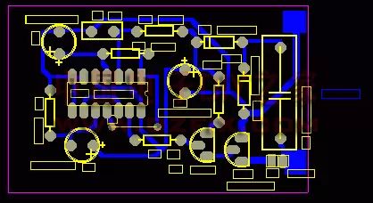
The schematic diagram is as follows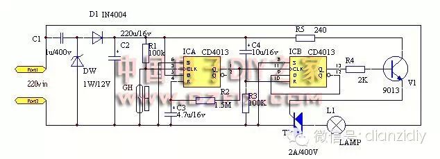 PCB diagram shown below