The design of PCBs is closely related to the production and subsequent use of PCBs and PCBA. This article introduces the relationship between PCB molding, panel separation, and PCB design.01 Introduction to Molding and Panel Separation MethodsThe working panel is molded into a shipping panel, which is generally done using a board retrieval machine; the shipping panel is then molded into PCS, commonly using V-CUT, connecting the retrieval board and the stamp holes. Some simpler designs may use punching molding methods.1) Punching Molding is highly efficient but poses a significant risk of mechanical damage to the PCB and results in rough edges. Generally, simple single-layer boards will adopt this method, while most boards do not use punching molding.2) V-CUT Molding is specifically for the shipping panel, so the board factory will first mount the large working panel onto a milling machine, milling out the shipping panel and some internal slots before proceeding with the V-CUT process.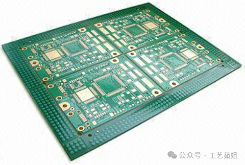 After component placement, V-CUT boards will be separated using a V-CUT cutting machine, manual separation tools, or purely manual separation methods.3) Retrieval Board Molding involves separating the shipping panel from the working panel, which will also retrieve the slots within the shipping panel; when separating the shipping panel into PCS, it also needs to be placed on the retrieval board machine for separation.
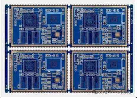 Retrieval boards need to be used with fixtures; working panel separation generally uses universal fixtures, while shipping panel separation often selects universal fixtures or custom fixtures based on PCB design and quantity requirements.4) Stamp Hole Molding is similar to the retrieval board molding method when the PCB factory separates the shipping panel, with the stamp holes completed at the drilling station. For separating the shipping panel into PCS, both retrieval machines and manual tools can be used.
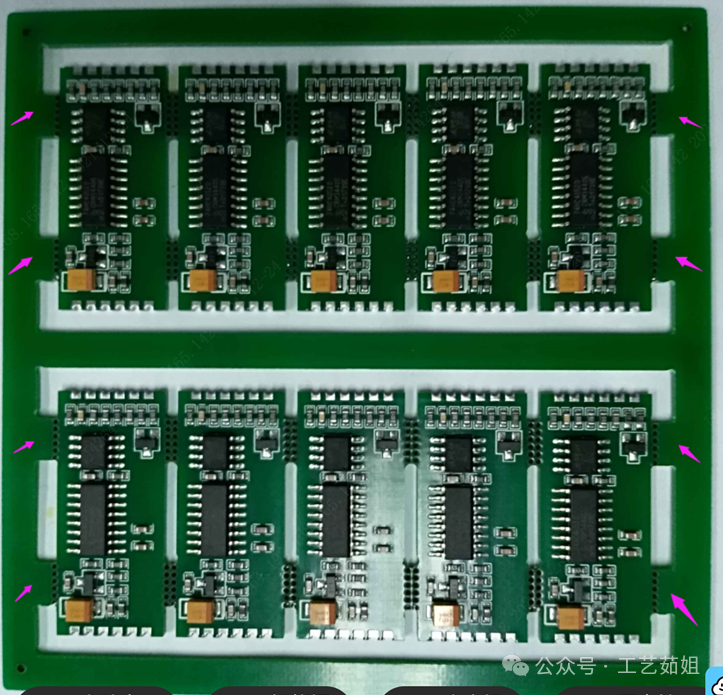 If the stamp hole method is ultimately used for mass production with a retrieval machine and fixtures, to enhance the strength of the PCBA and reduce drilling time, the PCB data can be modified to remove the stamp holes and shorten the connection length between PCS to improve reliability and efficiency.02 How to Choose a Reasonable PCS Connection Method1) Customer RequirementsSome custom products have specific requirements for the dimensional tolerances of the PCB, and the appropriate PCS connection method is selected based on these tolerances. The retrieval board method results in smoother edges and relatively small dimensional tolerances; V-CUT and stamp holes will have burrs after separation; punching molding results in rough edges and significant burrs.2) Process Equipment Requirementsa. Punching molding requires equipment and molds, and is suitable for very simple designs with large production volumes. If punching molding is to be used, the production line must have the corresponding equipment and mold-making capabilities or suitable mold suppliers.b. Retrieval molding requires a retrieval board machine and must be used with fixtures. If this separation method is to be designed, the appropriate equipment must be available, and the equipment capabilities must match the PCB design parameters, such as size, component height, etc.
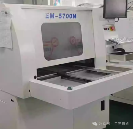 c. V-CUT generally requires a dedicated V-CUT separation machine, although some factories use simple tools for manual separation. To reduce the stress from manual separation, a separation machine should be used, and the production line must have the corresponding equipment.
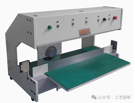 d. Stamp holes are generally separated manually. To reduce separation stress, a retrieval machine can be used for boards designed with stamp holes. V-CUT and stamp hole connections can be separated using professional separation machines or manually, offering strong adaptability.3) PCB Designa. PCB Size: Each separation device has size limitations for PCBs. The size of the PCB corresponds to which PCS connection method is suitable, and must meet the production line’s equipment capabilities. For connected designs or boards with waste edges, suitable sizes can be arranged based on equipment capabilities.b. Component Height on PCBA: Different separation machines have height limitations for components on the PCBA. If components on the PCB are tall, this must be considered when designing the PCS connection method.For example, the length limit of the retrieval machine’s milling cutter, the height limit of the V-CUT separation machine’s platform, etc.c. Distance from Components to Separation Area: Separation generates certain stress, and different connection methods and separation methods produce different stress levels. The appropriate PCS connection method can be selected based on the distance of components from the board edge.The method with the least separation stress is the retrieval board separation, as machine separation stress is less than that from manual separation.d. Component Types: Different types of components on the PCBA, such as fragile components near the board edge, require connection methods that minimize stress damage to fragile components during separation. If components extend beyond the board edge, V-CUT cannot be used for that edge.e. Waste Edge Design: Whether to add waste edges, whether to separate waste edges, and what method to use for separation must also consider the production line’s process conditions.f. Board Weight: The weight of the PCBA board also determines the connection method used. For small PCS sizes with heavy components, using V-CUT may result in many V-CUT strips, increasing the probability of board breakage during production.h. Board Thickness Design: Different thicknesses are suitable for different connection methods. For example, excessively thick boards are not suitable for stamp hole methods.i. Board Shape: The shape of the PCB also determines the connection method. For long strip designs with components protruding from the long edge, using V-CUT for separation may lead to insufficient PCB strength. For irregular PCBs, if the outermost edge length is short, V-CUT cannot be used.
 03 Common Defects in Molding and Separation StationsCommon defects at the molding station include: V-CUT upper and lower blade misalignment, V-CUT slot leakage, uneven V-CUT thickness, board breakage or process edge breakage, exposed copper damage, etc.;Common defects at the separation station include: severe burrs, damaged components, board breakage before separation or process edge breakage.
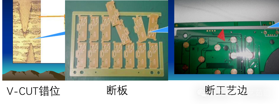 Design considerations include: reasonable V-CUT thickness specifications, reasonable connection area lengths, copper distance from the board edge should not be too close, fragile components should not be too close to the board edge, and reasonable design of stamp hole sizes and distances, etc.Disclaimer:This article is based on personal experience and is for reference only. If there are omissions or content beyond my experience, discussions are welcome; images are sourced from the internet.