MIPI (Mobile Industry Processor Interface) is a standard defined for mobile devices such as smartphones, tablets, laptops, and hybrid devices. Its commonly used physical (PHY) layers are MIPI D-PHY and C-PHY.
MIPI D-PHY: It is more commonly used in smartphone cameras and displays due to its flexibility, high speed, low power consumption, and low cost. It provides definitions for DSI (Display Serial Interface) and CSI (Camera Serial Interface) at the physical layer, using a differential clock and 1-4 pairs of differential data lines to transmit data.
MIPI C-PHY: C-PHY does not have a synchronized clock; instead, the clock is embedded within the data, achieving high throughput performance through bandwidth-limited channels, such as connecting displays and cameras to application processors. It provides PHY for the MIPI Camera Serial Interface (MIPI CSI-2) and MIPI Display Interface (MIPI DSI-2) ecosystem, helping designers extend their implementations to support various higher resolution image sensors and displays.
1. PCB Layout Requirements for MIPI Interfaces
1. Keep away from interference sources to prevent other signals from affecting the transmission rate and signal quality.
2. All display interfaces (whether in connector or FPC form) should be placed as close to the edge of the board as possible for easy plugging and unplugging.
3. The distance between the main chip and the display interface should not be too far; try to minimize the trace length, following high-speed signal routing guidelines.
4. If the PCB has structural requirements, placement should strictly adhere to those structures.
2. PCB Wiring Requirements for MIPI Interfaces
1. Reference Layer: To suppress electromagnetic radiation, MIPI differential lines should be routed as close to the GND plane as possible, ensuring that traces do not cross splits; otherwise, it may cause discontinuity in differential line impedance and increase external noise affecting the differential lines. If routed on the outer layer, ensure proper grounding or increase spacing from other signals.
2. Grounding: MIPI traces can be grouped with ground, with a GND via every 150 mils. If space permits, single-group grounding is preferable.
3. Minimize the number of vias for MIPI signal differential lines; vias can cause discontinuity in line impedance. If vias are necessary for layer changes, ensure consistency in differential vias and arrange a return ground via nearby for signal return.
4. Interference Principles: MIPI signal lines should be kept away from other high-speed signals (such as parallel data lines, clock lines, etc.), especially from interference sources like switching power supplies.
The PCB design wiring considerations for the MIPI-DPHY interface are shown in Table 1 below:
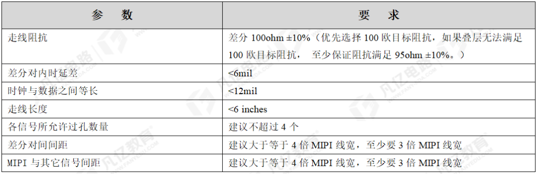
Table 1: PCB Design Wiring Considerations for MIPI-DPHY Interface
The PCB design wiring considerations for the MIPI-CPHY interface are shown in Table 7-8 below:
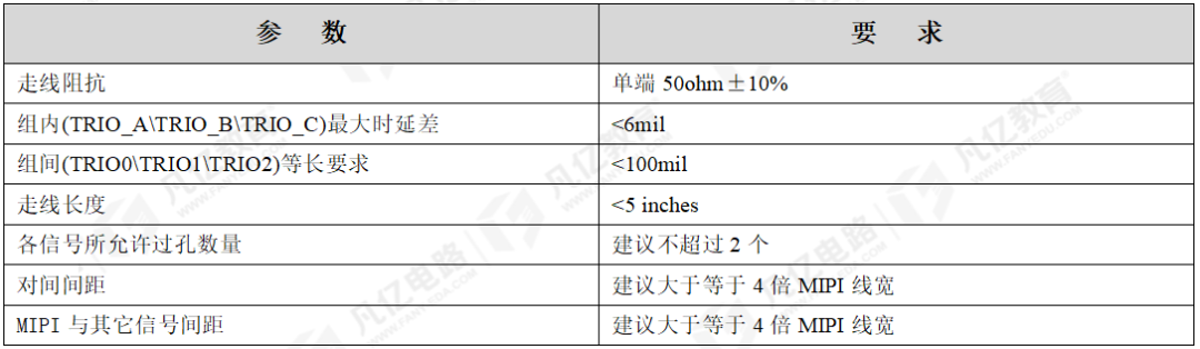
Table 2: PCB Design Wiring Considerations for MIPI-CPHY Interface
It is also recommended to add ground vias in the following locations in the BGA area, as shown in Figure 1.
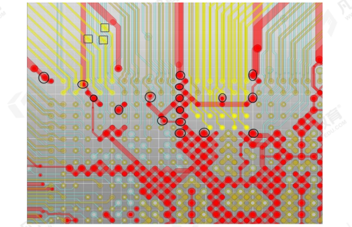
Figure 1: Addition of Ground Vias Under the BGA Area
Senior EMC Engineer’s Rectification Methodology
2025-08-21
Comprehensive Guide to PCB Electromagnetic Compatibility Design: Solving EMI and EMS Issues with a Systematic Approach
2025-08-19
Dissecting the Two Core Testing Methods of EMC: Radiated Emission and Conducted Emission
2025-08-16

Recurring EMC Issues? Implement These Three Steps in Your Project, and They Will Likely Cease
2025-08-14
EMC Failure Rectification Ideas and Practical Solutions
2025-08-12