 Artificial synapses are promising fundamental components in the field of neuromorphic computing, providing new pathways to overcome the inherent limitations of the von Neumann architecture. Compared to traditional memristors controlled by electricity, optically controlled synaptic devices are attracting widespread attention due to their unique advantages. This study demonstrates, for the first time, an all-optical synaptic function based on the bidirectional optical response characteristics of two-dimensional platinum diselenide (PtSe2) layers. Wafer-level two-dimensional PtSe2 layers, fabricated via chemical vapor deposition (CVD), exhibit unique photoconductive responses: a positive photoconductive effect under long-wavelength light (625-940 nm) and a negative photoconductive effect under short-wavelength light (405 nm). This tunable wavelength characteristic enables the integrated two-dimensional PtSe2 layers on flexible substrates to exhibit complete optical synaptic behavior, including wavelength-dependent excitatory postsynaptic current (EPSC) and inhibitory postsynaptic current (IPSC), paired-pulse facilitation (PPF) effects, as well as reversible switching between short-term/long-term potentiation (STP/LTP) and short-term/long-term depression (STD/LTD). Even under severe mechanical deformation conditions, devices based on two-dimensional PtSe2 layers can fully maintain these synaptic characteristics, successfully achieving basic logic operations and Pavlovian associative learning demonstrations. Further studies indicate that wafer-level two-dimensional PtSe2 arrays constructed on different substrates exhibit excellent optical pattern recognition, information retention, and enhancement capabilities, with minimal inter-device variation. These findings provide new insights for developing ultra-thin all-optical neuromorphic hardware, with mechanical reconfigurability showcasing broad application prospects.
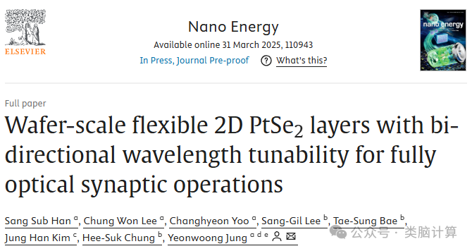
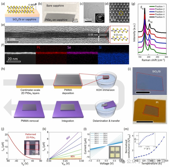 Figure 1(a) Schematic diagram of few-layer two-dimensional PtSe₂ on the growth substrate, highlighting its van der Waals gap along the c-axis.(b) Physical images of a centimeter-sized bare sapphire wafer (top) and a two-dimensional PtSe₂ grown sapphire wafer (bottom).(c) Plan-view transmission electron microscopy (TEM) image of two-dimensional PtSe₂ and selected area electron diffraction (SAED) pattern (inset shows (100) and (110) crystal plane calibration).(d) High-resolution scanning transmission electron microscopy (HR-STEM) image and overlaid atomic structure model (purple: platinum atoms, yellow: selenium atoms).(e) Cross-sectional STEM image of two-dimensional PtSe₂ (left) and corresponding atomic model (right), showing a 0.55 nm van der Waals spacing.(f) Cross-sectional energy dispersive spectroscopy (EDS) elemental distribution maps of Pt, Se, and Si.(g) Raman spectrum of two-dimensional PtSe₂ (Eg peak: 180 cm⁻¹, A1g peak: 207 cm⁻¹).(h) Schematic diagram of the PMMA-assisted transfer process.(i) Physical images of two-dimensional PtSe₂ transferred to SiO₂/Si (top) and PI substrate (bottom) (scale bar: 1 cm).(j) Transfer characteristics curve (Ids-Vg) of two-dimensional PtSe₂ field-effect transistors (FET), with inset showing device structure.(k) Output characteristics curves (Ids-Vds) under different gate voltages (Vg=-80 to 80 V).(l) Temperature-dependent current-voltage (I-V) characteristics curve (inset shows physical image of the tested device).(m) Normalized conductivity as a function of temperature curve (inset shows Arrhenius fitting, activation energy Ea=116 meV).
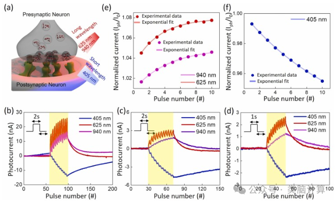
Figure 2(a) Schematic diagram of bio-inspired multi-wavelength optical synaptic operation.(b-d) Wavelength-dependent synaptic behavior under different electrodes (Au/PtTe₂) and pulse conditions (1s/2s intervals):(b) Response of gold electrode devices under 2s pulse intervals.(c-d) Response of PtTe₂ electrode devices under 1s and 2s pulse intervals, respectively.(e-f) Exponential fitting curves of normalized photocurrent:(e) Enhancement characteristics under long wavelengths (625/940 nm).(f) Suppression characteristics under short wavelengths (405 nm).
 Figure 3Synaptic plasticity characteristics under three sets of wavelengths (625 nm: a-d; 940 nm: e-h; 405 nm: i-l):Column 1: Changes in EPSC/IPSC under double-pulse stimulation and PPF index calculation.Column 2: PPF index decay curves dependent on pulse intervals (Δt).Column 3: STP-to-LTP/STD-to-LTD conversion induced by pulse counts (5-20 pulses).Column 4: STP/LTP or STD/LTD transitions regulated by pulse frequency (0.1-1 Hz).
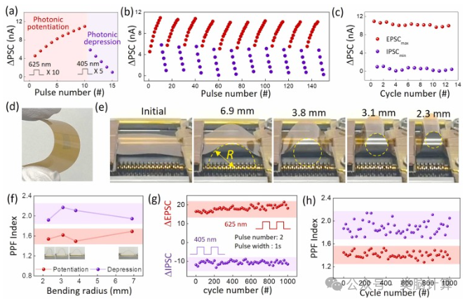 Figure 4(a) Synaptic plasticity of flexible two-dimensional PtSe₂/PI devices under alternating stimulation at 625 nm (10 pulse enhancement) and 405 nm (5 pulse suppression).(b) Retention of characteristics under continuous enhancement/suppression pulses.(c) Stability of maximum EPSC (EPSCmax) and minimum IPSC (IPSCmin).(d) Physical image of the flexible device in a bent state.(e) Sequential images at different bending radii (R=2.3 to 6.9 mm).(f) Effect of bending radius on PPF index (red: 625 nm enhancement, purple: 405 nm suppression).(g) Durability of ΔEPSC/ΔIPSC over 1000 bending cycles.(h) Stability of PPF index under long-term bending tests.
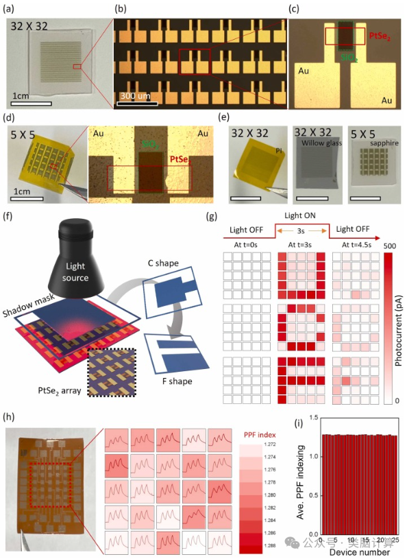 Figure 5(a-c) 32×32 PtSe₂ array on sapphire wafer:(a) Optical microscope (OM) image of the entire array.(b) Local magnification showing multiple device patterns.(c) High-magnification image of a single device (active channel within the red box).(d) Fabrication of a 5×5 array on a flexible PI substrate (right: schematic diagram of device structure partitioning).(e) Physical images of PtSe₂ arrays with different substrates/densities (scale bar: 1 cm).(f) Schematic diagram of optical pattern recognition experiments using the “U/C/F” mask.(g) Optical pattern recognition and short-term retention characteristics (three columns respectively show: dark current, reconstructed pattern under 625 nm light, image retention 1.5 seconds after light termination).(h) Physical image of the flexible array (left) and heat map of enhanced characteristics of its 25 devices (right).(i) Statistical histogram of PPF indices for all devices (mean 1.28, standard deviation 0.006).
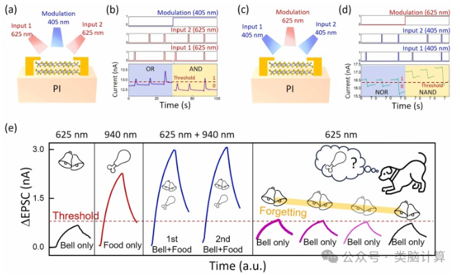 Figure 6(a-d) Implementation of wavelength-selective Boolean logic gates:(a) OR/AND logic schematic (two 625 nm inputs + 405 nm modulation).(b) OR/AND operation experimental results (threshold current: 12.9 nA).(c) NOR/NAND logic schematic (two 405 nm inputs + 625 nm modulation).(d) NOR/NAND operation verification.(e) Pavlovian associative learning demonstration: “training-memory-forgetting” process controlled by 625 nm (bell) and 940 nm (food) light pulses.
Below is a summary of the core points of this research:
-
Bidirectional Wavelength Tunable Optical Synaptic Characteristics Wafer-level two-dimensional PtSe₂ layers fabricated via chemical vapor deposition (CVD) exhibit unique bidirectional photoconductive responses: long-wavelength light (625-940 nm) induces positive photoconductivity (excitatory postsynaptic current EPSC), while short-wavelength light (405 nm) triggers negative photoconductivity (inhibitory postsynaptic current IPSC). This wavelength dependence enables all-optical control of synaptic plasticity, including paired-pulse facilitation (PPF) and transitions between short-term/long-term potentiation (STP/LTP) and short-term/long-term depression (STD/LTD).
-
Flexible Substrate and Mechanical Stability Devices based on PtSe₂ integrated on a polyimide (PI) flexible substrate maintain complete synaptic functionality even after severe mechanical bending (radii as small as 2.3 mm) and 1000 cycles of deformation. This mechanical robustness opens possibilities for wearable neuromorphic hardware and reconfigurable optoelectronic devices.
-
Wafer-Level Arrays and Pattern Recognition Applications Wafer-level PtSe₂ synaptic arrays (e.g., 32×32 arrays) have been successfully fabricated on various substrates such as sapphire, PI, and Willow glass. Through optical pattern stimulation (e.g., the letter “U/C/F”), the arrays demonstrate uniform optical pattern recognition, information retention, and enhancement capabilities, with minimal inter-device variation (PPF index standard deviation of only 0.006), validating the feasibility of large-scale integration.
-
Realization of All-Optical Neuromorphic Functions Boolean logic operations (OR/AND/NOR/NAND) and Pavlovian associative learning have been achieved solely through optical pulse control. For example, 625 nm (bell) and 940 nm (food) light were used to simulate conditioned/unconditioned stimuli, successfully demonstrating the entire process of biological associative learning: “training-memory-forgetting” without the need for electrical signal intervention.
-
Analysis of Interface Charge Trapping Mechanism The study reveals the physical origin of bidirectional photoconductivity: short-wavelength light (405 nm) activates interface-adsorbed molecules (e.g., oxygen) that trap electron-hole pairs, leading to negative photoconductivity; while long-wavelength light promotes carrier generation, resulting in positive photoconductivity. Vacuum control experiments validate the environmental dependence, providing theoretical guidance for material design.
These findings pave the way for the development of ultra-thin, all-optical, and mechanically reconfigurable neuromorphic hardware, particularly suitable for next-generation artificial intelligence systems requiring high bandwidth, low power consumption, and flexible integration.