Previously, it was explained that when external registers need to be added, the bus interconnection module must be changed. In the bus interconnection module, each register has a wire connected to the bus interconnection module for reading data and enabling signals. If there are relatively few registers, it seems there is no problem. But what if there are thousands or tens of thousands of external registers? The circuit in this case is truly unimaginable; it would be practically impossible to create because the area required would be too large. Just imagine a multiplexer with thousands or tens of thousands of inputs; how could that be designed?
Therefore, a true SOC cannot be designed as we previously discussed, considering each register individually. Instead, we must consider the overall system. We know that the SOC actually drives a module, such as the serial port module, SDRAM module, SPI module, etc. However, to drive a module, the registers of that module need to be controlled. At this point, the enable signal does not need to be considered for each register of the module but rather for the module as a whole. Similarly, reading data does not need to be considered for each register of the module, but for the module itself. Following this approach, the design of the enable signal circuit and the read data circuit becomes simpler because there are only a limited number of modules in an SOC. This makes the bus interconnection decoding design much easier. The remaining task of operating the corresponding registers can be left to the module itself.
The bus interconnection module determines which module an address belongs to based on the address sent by the CPU, then enables the corresponding module’s enable signal and connects the input data line to the module’s read data line. The module detects the enable signal and, based on the address signal sent by the CPU, determines which register of its own to operate on and then performs the operation. This simplifies the design of the bus interconnection.
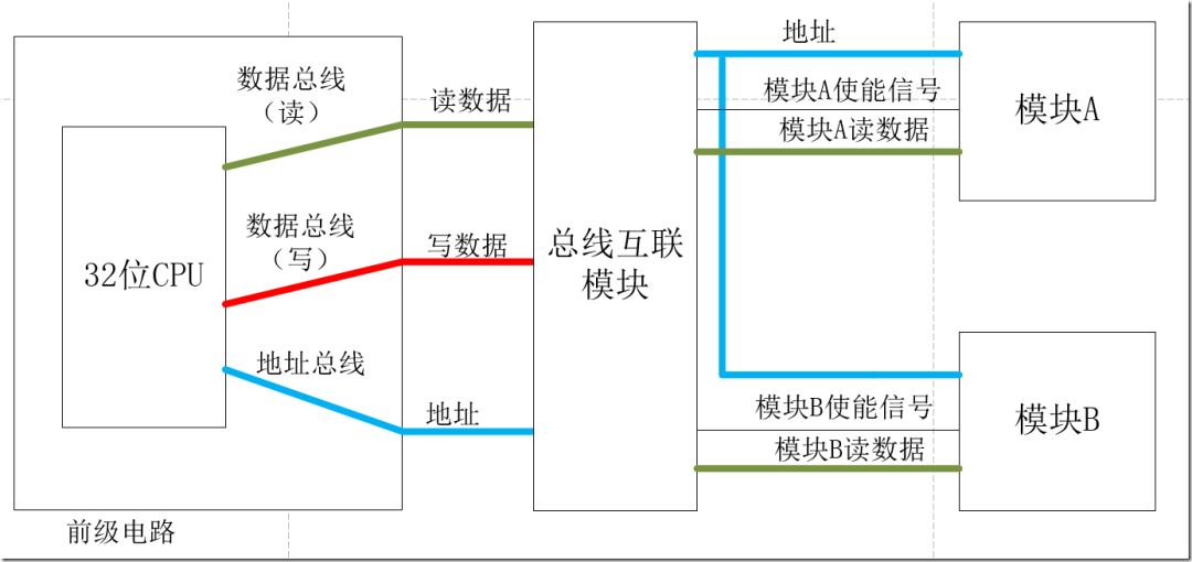
From the above diagram, we can understand what was said earlier. At this point, the bus interconnection module does not care how many external registers there are; it only cares about how many modules there are. It allocates addresses continuously to these modules so that each module will receive a portion of continuous addresses. When the bus interconnection module detects that the CPU‘s address is within a certain module’s address range, it enables the corresponding module’s enable signal and connects the module’s read data to the CPU‘s read data.
Assuming there are 8 modules and the bus is 32 bits wide. The address range is from 0x00000000 to 0xffffffff. If we evenly distribute the 4G address space among each module, then each module will be allocated 512M of address space. For example, for the first module, the address range is from 0x00000000-1fffffff. When the address sent by the CPU is 0x00856840, it falls within the address range of the first module, so the enable signal for the first module will be valid.
Next, let’s take a look at the memory mapping of STM32.
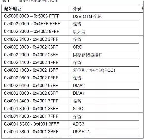
It can be seen that the STM32 is also designed in the above manner. For example, for USART1, the address range is from 0x40013800 to 0x40013bff. The size of the address range is 1K bytes. But does this module have 256 registers (32 bits)? Let’s take a look at the register address of USART.
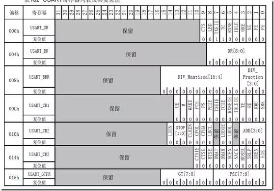
From the above image, it appears that there are only 7 registers, but the address space is 256, which means there is a waste of 249 registers of space. Yes, there is indeed waste, and that is unavoidable because you want to simplify the circuit for address decoding in the interconnection bus, so many register addresses will be wasted. This is the trade-off.
For the processor, the module addresses are fixed, and the set of module addresses is also fixed. There is not much to study in this regard, but for an SOC, the set of module addresses must be allocated by ourselves.
Using Vivado software, create a new ZYNQ processor and then add a GPIO peripheral IP. The schematic is shown below:
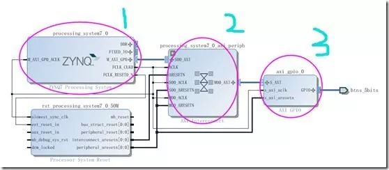
1 is the ZYNQ processor, 2 is the bus interconnection module, and 3 is the GPIO module. At this point, check the peripheral module address allocation.
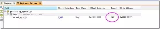
It can be seen that the address allocation for this GPIO peripheral is from 0x41200000-0x4120ffff. The size is 64K bytes. This 64K is the address range for this peripheral. Of course, we can change this size.
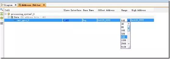
However, when changing, it seems that the selected values have a pattern. If you convert these values to binary, you can see that regardless of the value, the converted binary only has the highest bit as 1 and all others as 0. Moreover, if you calculate the address ranges of the register for the modules of STM32, you will find that the pattern in the size of the address range is the same as that in Vivado; only the highest bit is 1 and all others are 0. This greatly simplifies the design of the decoding circuit for the interconnection bus.
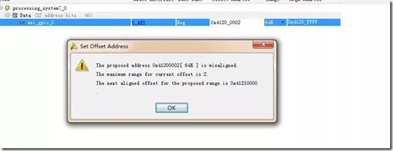
If we change the value of Offset_Address, we may encounter the following error. This indicates that the starting address of the module cannot be set arbitrarily, but must meet certain requirements. However, for ZYNQ development, the Vivado software will automatically generate the starting address for us.
However, if we are designing an SOC system ourselves, we need to consider how to allocate the addresses for the modules because this affects the simplicity of our interconnection bus decoding design. Therefore, address allocation for the SOC is not a trivial matter.