Click on “High Technology and Industrialization” above to subscribe!
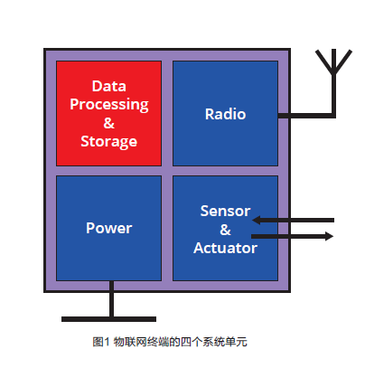
**Sensors and actuators** are crucial components of IoT systems. Smart sensors form the perception layer of IoT systems and are the most direct system units for data collection in IoT systems. An independent IoT terminal generally consists of sensors, a data processing unit (processor plus memory), a power management unit, and a wireless communication unit. In such terminals, the data collected by sensors is processed by the data processing unit and transmitted to the cloud via the wireless communication system, achieving connectivity with the entire network. The requirements for sensors in IoT applications include: device miniaturization, functional integration, low cost, and mass production. Among these, low cost and mass production are directly related. The MEMS technology derived from silicon-based integrated circuit manufacturing can meet these requirements and has become the mainstream production technology for miniature sensor technology in the IoT era.
Widely Used MEMS
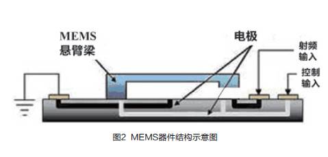
MEMS stands for Micro-Electro-Mechanical Systems. It has two characteristics: first, the device size is at the micro or nano scale; second, it typically has a suspended moving part to realize sensing or actuation functions, such as the cantilever beam shown in Figure 2. When the motion state of the cantilever beam changes, the designed electromechanical coupling device converts mechanical motion into electrical signals. There are many methods for electromechanical coupling, for example, the cantilever beam and the electrodes below it can form a capacitor, which can produce an output voltage signal that provides information about the motion of the cantilever beam. By attaching thin film materials that can perceive external environments, known as sensing layers, various sensors can be manufactured. For instance, motion sensors can detect pressure, acceleration, motion direction, distortion, flow, wind force, etc. A microphone, which senses sound waves, is a common type of motion sensor that has found widespread application in mobile phones and portable devices. When a light-sensitive layer is attached to MEMS, it can convert light into heat, changing the shape of the cantilever beam, thus forming light-sensitive sensors, infrared image sensors, etc.
MEMS technology can also use electrical signals to control the movement of the cantilever beam, producing actuators, such as micro motors, micro switches, micro pumps, inkjet print heads, etc. The MEMS speakers widely used in mobile phones are a typical example of actuators. MEMS can also be used to create electro-optical devices, such as micro mirrors, micro projectors, and micro light shutters, used in optical systems. Another type of device manufactured using MEMS technology utilizes the mechanical resonance of the cantilever beam to create high-frequency filters, which are expected to replace surface acoustic wave filters. Additionally, there are energy harvesting devices that convert mechanical motion energy into electrical energy for storage.
As products, MEMS sensors appeared relatively late. In the 1980s, the first MEMS sensor for engine control was produced by packaging a silicon cantilever beam structure on glass. In the 1990s, MEMS accelerometers began to be used in automotive airbags; moreover, MEMS pressure sensors were applied in blood pressure monitors; and inkjet print heads made using MEMS technology became the first widely used consumer MEMS actuators. From 2000 to 2010, MEMS sensors and actuators were significantly promoted, leading to the emergence of tire pressure sensors for measuring tire pressure, gyroscopes for monitoring the horizontal and vertical movements of cameras and mobile phones, MEMS microphones and speakers, MEMS switches, infrared image sensors, fingerprint recognition sensors, and many other products.
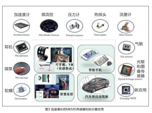
Since 2010, driven by the demand for IoT technology, various MEMS sensors and actuators have been widely applied in wearable systems, virtual reality products, smart homes, smartphones, smart manufacturing, automobiles, and autonomous driving (Figure 3). Products include various motion sensors and actuators (gyroscopes, micro pumps, headphones, headsets, accelerometers, pressure gauges, flow meters, microfluidic devices, etc.), gas-sensitive, humidity-sensitive, and light-sensitive sensors, infrared imaging devices, etc. There are already more than a dozen MEMS device products used in smartphones, including 9-axis gravity accelerometers, microphones and speakers, antenna switches, timers, camera autofocus systems, micro mirror projectors, temperature-humidity-pressure-gas sensors, biosensors, and in the future, energy harvesting devices, infrared night vision devices, ultraviolet sensors, ultrasonic sensors, radiation detection sensors, etc. may also be introduced.
CMOS-Based Manufacturing Technology
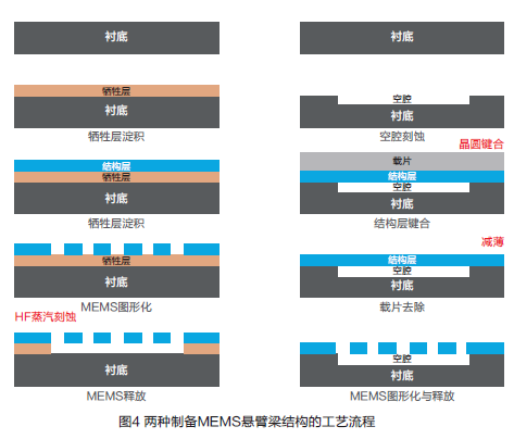
MEMS manufacturing technology is derived from CMOS integrated circuit manufacturing technology. Over the past 50 years, CMOS integrated circuit manufacturing technology has developed rapidly, becoming the most precise and complex manufacturing technology in history. In terms of device size, the line width has shrunk from 1 micron in the 1970s to the current 20 nanometers, greatly increasing the number of devices per unit area of silicon substrate. In terms of device patterning, the process capabilities of CMOS technology far exceed the requirements for MEMS device manufacturing. It can be said that CMOS integrated circuit manufacturing technology has laid a solid foundation for MEMS manufacturing. However, on the other hand, MEMS manufacturing processes have characteristics that differ from CMOS manufacturing. First, it has a unique cantilever beam formation process. There are two types of cantilever beam formation processes available: one uses sacrificial layer processes, and the other uses wafer bonding processes. Figure 4 (left) shows a schematic diagram of the process for forming a cantilever beam using the sacrificial layer process. The specific approach involves depositing a sacrificial layer on the silicon substrate surface, such as a silicon dioxide layer, structural layer, or polysilicon layer. Then, special process designs are used to expose the sacrificial layer through photolithography, etching, and chemical mechanical polishing (CMP), etc. The sacrificial layer is then corroded away using chemical solvents (wet etching) or chemical vapor (dry etching), leaving the structural layer suspended to form the cantilever beam. Figure 4 (right) illustrates the process for forming a cantilever beam using wafer bonding. The specific approach involves first forming a cavity beneath the cantilever beam on the silicon substrate, then bonding the structural layer wafer surface down to the substrate wafer. The structural wafer is then thinned from the backside, retaining only the thickness required for the cantilever beam. Photolithography, etching, and other CMOS patterning processes are then used to form the cantilever beam. The difference between the two technical solutions is that the former’s process is relatively simple, and except for the need to introduce special vapor etching equipment during vapor etching, it can mostly use existing CMOS industrial equipment, making it compatible with CMOS manufacturing. The wafer bonding process, however, requires the use of wafer bonding equipment, thus increasing the technical complexity and, consequently, manufacturing costs. Its advantage is that the quality and process consistency of the cantilever beam are high. In the sacrificial layer process, the structural layer is formed from high-temperature deposited polycrystalline materials, which inevitably retain stress within the layer. As a result, fluctuations in the conditions for thin film growth can easily lead to uniformity issues both within and between wafers, potentially reducing yield. The structural layer formed using the bonding process is made of single-crystal materials, which do not have the stress associated with high-temperature growth, resulting in better material performance consistency and significantly benefiting yield improvement.
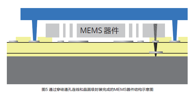
Another aspect in which MEMS processes differ from CMOS processes is their special packaging requirements. For CMOS, when devices complete multi-layer interconnections through interconnect methods, they can be packaged through side wire bonding, flip chip soldering, or multi-dimensional (2.5D/3D) packaging based on through-silicon vias (TSV) technology, and then filled with encapsulation materials. In contrast, for MEMS, the cantilever beam structure must be able to move freely; thus, it cannot be packaged like CMOS with filling materials but must use a cap sealing method, enclosing components like the cantilever beam with a cap. No filling material is injected inside the cap. Especially for motion-type MEMS devices, it is necessary to maintain a vacuum inside the cap. Therefore, MEMS packaging brings significant process complexity and cost increases. When using single-chip cap sealing processes, packaging accounts for over 70% of the manufacturing cost of vacuum-sealed MEMS. One method to reduce costs is to adopt wafer-level packaging, which designs and manufactures a cavity on a single silicon wafer, forming a cap wafer that is then placed over the device wafer to achieve wafer-level vacuum packaging. To match wafer-level packaging, the electrical leads must also be considered. Figure 5 shows a schematic diagram of a MEMS device structure completed through through-silicon via connections and wafer-level packaging.
Opportunities and Challenges
MEMS technology has a very broad application prospect, especially with the advent of the IoT era, as only MEMS can meet the requirements for sensors and actuators in IoT applications. First, the size of MEMS completely meets the miniaturization requirements of IoT applications. Second, the compatibility of MEMS technology with CMOS technology makes it easy to meet the intelligent requirements for sensors and actuators in IoT. Using the same production line, both CMOS integrated circuits and MEMS devices can be manufactured simultaneously, achieving heterogeneous integration. Heterogeneous integration can be accomplished by manufacturing both on the same chip and interconnecting them, or by manufacturing on different wafers and integrating them into the same system through 2.5D or 3D packaging. The third advantage is MEMS’s advantage in energy consumption. IoT applications have much stricter power consumption requirements than other application environments. The sensing and actuation methods of MEMS make it a low-energy-consuming device, making it the most likely technology to meet the power consumption requirements of IoT. Another advantage is its ability to meet the quantity requirements for sensors/actuators in IoT applications. Silicon-based integrated circuit technology can manufacture tens of thousands of MEMS sensors on a single wafer while maintaining low manufacturing costs. Thanks to the R&D investment during the development of CMOS manufacturing technology, the equipment and manufacturing processes required for MEMS manufacturing already exist. Only minor adjustments and developments are needed for MEMS production. In fact, the production lines currently used for MEMS manufacturing are mainly those that have been phased out from mainstream CMOS product manufacturing, such as 8-inch lines. Using these production lines can meet the mass production requirements while reducing the manufacturing cost of each MEMS to the level required for consumer products.
It is estimated that by 2018, the global MEMS direct market could reach 1.2 billion dollars, and with the indirect market, the total could exceed 3.3 billion dollars. Moreover, it will grow at a rate of over 40% per year. Due to the diverse application types in the MEMS market and the diversification of product production technologies, opportunities arise for small and medium-sized enterprises. Particularly, companies with prior technical accumulation will discover opportunities in the aforementioned market, achieving rapid growth. However, on the other hand, the development of MEMS production technology and the growth of enterprises also face some unique challenges. First, the segmentation of the MEMS market is prominent, making the total demand for a single product much smaller compared to integrated circuit products, while the investment in MEMS product production lines is relatively large, resulting in high investment risks and long investment return cycles, which somewhat limits the development of the MEMS industry and enterprises. To address the difficulties faced by small and medium-sized enterprises in industrial technology development and gaining investor confidence, promoting the agglomeration and development of the national and local MEMS industry, a feasible measure is to establish public technology R&D platforms to provide process R&D and pilot services for small and medium-sized enterprises, aiming to reduce investment blindness and enhance the survival capability of startup companies.
In recent years, the Institute of Microelectronics of the Chinese Academy of Sciences has established a complete MEMS process pilot line, using industry-standard production equipment to provide R&D services for enterprises, achieving good social benefits. It is believed that through the joint efforts of the state, localities, and enterprises, and practicing the concept of industry-university-research cooperation, we will be able to overcome the difficulties encountered in industrial development and promote the rapid development of the MEMS industry, promptly meeting the rapidly growing demand for sensors and actuators in IoT technology.
(Author Affiliation: Zhao Chao, Institute of Microelectronics, Chinese Academy of SciencesJiao Binbin, University of Chinese Academy of Sciences)
MoreCopyright Statement:
The text, images, etc. published by this WeChat public account are owned by the editorial department of “High Technology and Industrialization.” For authorized cooperation, please contact [email protected]

Please subscribe to the “High Technology and Industrialization” magazine
Address: 33 Xihuan West Road, Zhongguancun, Haidian District, Beijing (100190) Phone: 010-82627674
Fax: 010-86267674 Email: [email protected]
Website: http://www.hitech.ac.cn
12 issues a year, 58 yuan per issue, annual subscription price 696 yuan
Postal code: 82-741
Publication number: ISSN1006-222X CN11-3556/N