01IntroductionTime flies. When I first started working, I found that I had a lot to say about the topic of PCB. Perhaps over the years, I have encountered many things related to PCBs. From initially disassembling circuits to designing my own boards, from foreign AD to domestic Lichuang EDA, from double-layer boards to four-layer and six-layer boards, and from low-speed to high-speed board design, I have many feelings.02Corporate CultureMy first encounter with PCBs was when I just started elementary school, nearly a decade ago. At that time, my family lived in a rural area in East Henan, and my neighbor opened a waste recycling station where I could often rummage through many electronic products. The copper wires inside transformers were red, purple, green, and various colors, which I have not seen again. It was during that time that I discovered some boards from electronic products, filled with tiny components. I was very curious about how these boards could light up small bulbs and make small speakers sound. Looking back now, that was a PCB.One afternoon, I had a sudden idea. I disassembled many components from a small board and connected them haphazardly to a small light bulb, then reached for the socket, foolishly thinking that my ridiculous action could light up the bulb. That year, holding the bulb felt like grasping the entire summer. What happened next left me frozen in place for a long time. I only remember the socket emitting a blinding light, and my body felt like it was frozen in place. I could clearly hear my heart racing, as if it wanted to jump out of my chest. This bright flash left a strong shock and fear in my young heart, so much so that even after more than a decade, despite many memories fading, this scene remains vivid in my mind.I encountered PCBs again when I was about to enter middle school. I loved music, and my father bought me a Bluetooth speaker around 2012, when brands like Gionee, Bird, and Nokia were still popular. One day, the little speaker broke down, so I decided to take it apart. I remember that it was just a wire that had broken. At that time, I hadn’t played with a soldering iron yet, so I used tape to stick the pins together, and it worked. The mainboard of that speaker was just like what we see now, with surface-mounted components, a green solder mask double-layer board, and an SOP8 Class D amplifier chip. This little speaker was the spark of my interest, and from that moment on, I developed a fondness for amplifiers.Time flew by quickly, and before I knew it, I was in high school. High school in Henan is tough, with early and late self-study sessions consuming almost all my spare time. However, on weekends, I still had some time to play with these things. I started using Taobao and found the beginner-friendly TDA2030 small amplifier, took a saw to cut wood, searched for speakers, and assembled my first 8-inch speaker. That summer, I was very happy, listening to the sound of the speaker I made, feeling particularly refreshed.Fast forward to college, which was when my knowledge accelerated. I spent a lot of time learning the fundamentals of analog and digital circuit knowledge, and later I also learned to code. However, in subsequent competitions, I gradually shifted towards hardware. That year, PCB manufacturers started competing fiercely; previously, it would cost over a hundred yuan for a board, but now it was practically free. Although the term ‘competing fiercely’ sounds harsh, it must be said that these two years greatly promoted the development of us college students in the hardware PCB field. During college, I participated in many competitions and won numerous national and provincial awards and patents, mainly focusing on hardware circuit PCB design, which helped me accumulate valuable experience for my future job.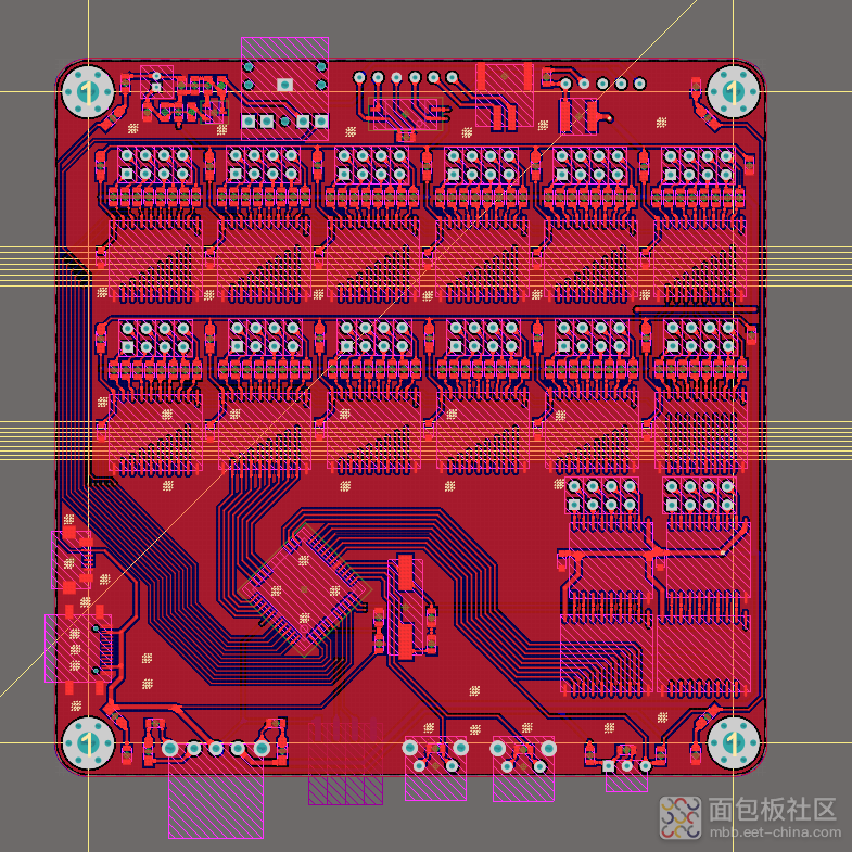 This is my first PCB drawn using AD; it doesn’t look too much like a first attempt, right?
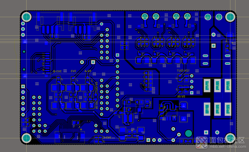 This is a driver board I drew for a later competition.Now, I have joined an amplifier design company, and I really enjoy this job, which is also related to hardware design. Here, I started to pay attention to many points that I hadn’t noticed before, such as EMC, ESD, impedance, high speed, thermal analysis, etc. I have a term in my heart called ‘learning without end.’ In every new environment, I can learn new knowledge and gain new insights. Below, I will discuss a small portion of the related knowledge I have used in the past.03EDA SoftwareThe real design of a PCB must start with EDA software; without EDA software, there would be no PCB. There are many EDA software options we commonly use. For consumer products, PADs are more common, while Cadence is used more for high-speed multilayer boards. Similarly, there is a distinction between coastal and inland preferences. For college students and most companies without high-speed design or high-cost requirements, AD (Altium Designer) is still a popular choice. In the past two years, due to certain reasons, domestic EDA software has also gained attention, with excellent software like Lichuang EDA emerging.ADAltium Designer is a tool that most newcomers will use; it is a relatively complete and powerful EDA design tool. Even after using it for three or four years, I occasionally discover some useful features when communicating with colleagues. AD is very powerful, and in terms of some advanced features, domestic EDA cannot compare. The priority settings and shortcuts in AD can greatly enhance efficiency in the design process. Below are some collected shortcuts for reference.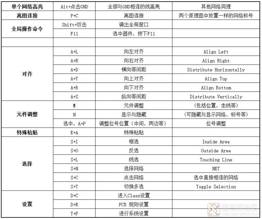
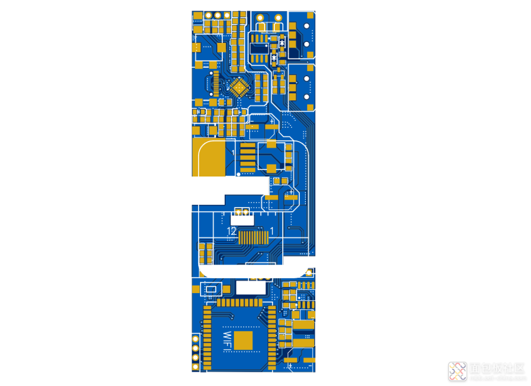 Lichuang EDAIn the current trend over the past two years, domestic EDA software has made significant strides, with Lichuang EDA being among the best in terms of ecosystem. Initially, I did not plan to use it, but due to its association with prototyping, I tried it once and found that its libraries and common features are sufficient for our daily design needs, and prototyping SMT and material procurement can all be completed in one go, which is something other EDA software cannot match.This is a PCB I quickly drew using Lichuang EDA, and I could preview a very realistic 3D simulation image through its built-in library.Can you tell what functions this irregular board has?However, there are also points to mention. Other older EDA software products have accumulated updates over many years. When facing professional EDA board-making requirements, it is still necessary to use software like Cadence or AD. In terms of some advanced features, domestic EDA still has a long way to go.03PCB Disassembly DIYAn hardware engineer must have disassembled a few small products. Throughout my growth, I have disassembled countless items, but I didn’t keep records early on. A few days ago, I disassembled a high-power lithium battery charger and wrote an article about it, which you can check out – Disassembly of a High-Power Lithium Battery ChargerIn this disassembled charger, many excellent designs can be seen. Large vias are beneficial for heat dissipation, and large areas of copper are conducive to smooth current flow, but its overvoltage and reverse connection protection are poorly designed, which is also the reason why this mainboard failed. This is worth our reference.
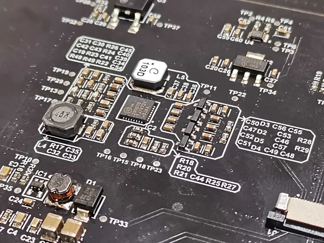
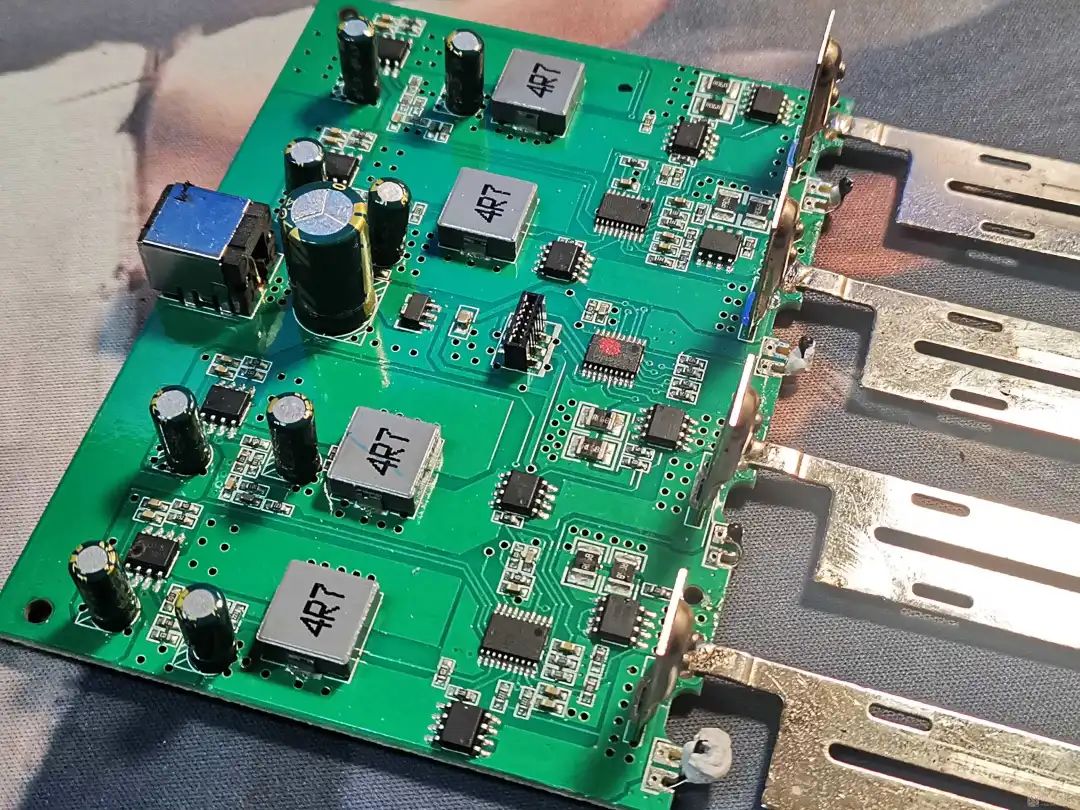 The following image is a partial diagram of a lithium battery charger I designed, and I also wrote an article to document it – High-Power Lithium Battery ChargerThis board very much aligns with the idea of high cohesion and low coupling. The circuit is divided into modules based on functionality, with 0-ohm jumpers between modules for one-time soldering and distributed debugging. In terms of silkscreen processing, it also aligns with personal aesthetics, making it easy to distinguish and observe.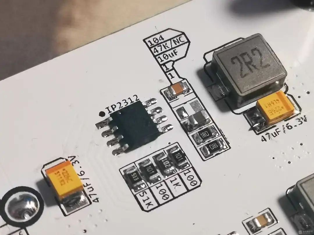
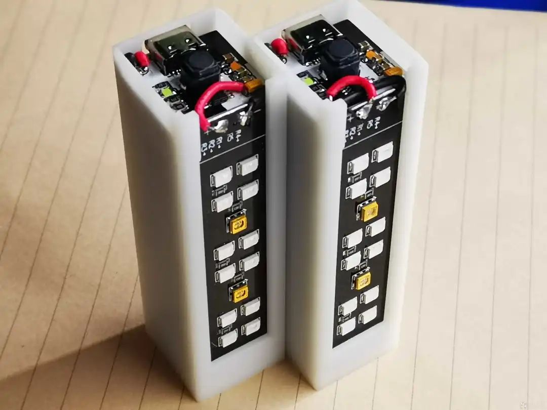 This little item was completed with both PCB and modeling. There is also an article introducing it – Portable UV Disinfection LampIn the process of making this product, the role of structure is reflected. The shape of a PCB in a product is definitely not arbitrary.The shape design is determined according to the drawings provided by the structure. Then, layout processing is performed within the PCB. In this board design, routing slots were reserved, considering the thickness of the PCB and the height of the components, among other information. Overall, there are many considerations when designing a good product.
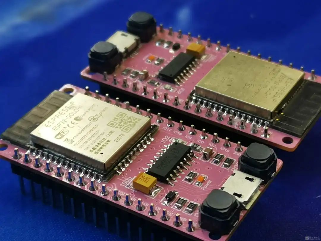 The following image is a core board of the ESP32-SOLO. When the industry launched pink solder masks, I immediately tried it out and printed a pink PCB.The following board is a driver board for a display, with MIPI signals routed as differential pairs, maintaining equal length for the differential pairs, grounding vias, and serpentine routing close to the terminals for impedance matching. Controlling these points should generally make simple differential impedance design not an issue.
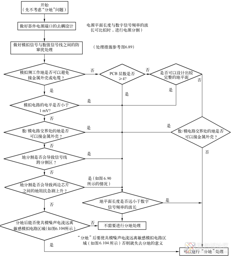
 04EMC DesignNext, I want to discuss advanced considerations for PCB design. In the development process of a product, it must go through EMC certification, so PCB EMC design is particularly important.EMC (Electromagnetic Compatibility) refers to the ability of electronic and electrical devices or systems to work normally in the expected electromagnetic environment according to design requirements. It is an important technical performance of electronic and electrical devices or systems, mainly including EMI (Electromagnetic Interference), EMS (Electromagnetic Susceptibility), and electromagnetic environment. It includes dozens of testing standards such as CE (Conducted Disturbance), RE (Radiated Disturbance), ESD (Electrostatic Discharge), EFT (Electrical Fast Transient), and SURGE.A PCB is like a miniature version of a complete product. It is the most worthy part of discussion in EMC technology, being the part of the device that operates at the highest frequency and is often the lowest level and most sensitive part. The EMC design of a PCB actually includes grounding design, decoupling, and bypass designs. A PCB with a good ground plane not only reduces the voltage drop caused by common-mode current but is also an important means of reducing loop area.Once a product’s PCB is designed, it can be said that the disturbance and resistance characteristics of its core circuit have basically been determined. To further improve its electromagnetic compatibility characteristics, one can only rely on filtering in the interface circuit and shielding of the enclosure to ‘surround and block’ it, which not only greatly increases the subsequent costs of the product but also increases the complexity of the product, reducing its reliability. A good PCB can solve most electromagnetic interference problems, as long as transient suppression devices and filter circuits are appropriately added during the layout of the interface circuit, most of the susceptibility and interference issues can be resolved. Enhancing electromagnetic compatibility in PCB routing does not incur additional costs to the final product. In PCB design, if product designers often focus only on increasing density, reducing space occupancy, simplifying production, or pursuing aesthetics and even distribution, while neglecting the impact of routing layout on electromagnetic compatibility, causing a large amount of signal radiation into space and creating interference, then this product will lead to numerous EMC problems. Many examples show that even with filters and components, these issues cannot be resolved, and ultimately, the entire board must be re-routed.A PCB with good EMC design must avoid common-mode interference currents flowing through the internal circuits of the product and direct them to the ground, low-impedance enclosure, or non-sensitive circuit areas within the circuit. Similarly, EMI noise source circuits within the PCB, such as clock generation circuits, clock transmission lines, switch power supply switching loops, high-frequency signal lines, etc., as well as the product’s EMI noise or common-mode voltage must also be isolated within the circuit, avoiding coupling with external circuits or cables to prevent radiation.In EMC design, consider the following points to avoid problems.Device partitioning and signal line partitioning ensure that digital devices are in one area, while analog devices or signal lines are in another area, and there is ground isolation between the top and bottom layers of the PCB to reduce crosstalk and radiation.In multilayer PCB design, it is recommended to set a local ground plane beneath the crystal oscillator. For two-layer boards, this method is particularly important, as standardized design will make subsequent troubleshooting much quicker.For multilayer boards with six or more layers, clock lines should not be routed long distances on the top or bottom layers. The maximum allowable length of surface clock lines should be 1/20 of the clock signal wavelength.Signal lines cannot be routed within 300 mils below the crystal oscillator and the driving circuit.TVS and similar protective devices should be placed at the signal entry point after the interface connector, close to the connector, and the protective device should be positioned between the protected device and the interface connector, so that the signal passes through the protective device before reaching the protected device.Avoid placing high dU/dt printed lines or devices at the edges of the PCB. If they must be placed at the edges for other reasons, a working ground line can be routed alongside the printed line, and this working ground line can be connected to the working ground plane through vias. Sensitive printed lines or devices placed at the edges of the PCB will create susceptibility issues.Eliminate a misunderstanding: do not think that radiation is directly caused by the crystal oscillator. In fact, the crystal oscillator is relatively small; it directly affects near-field radiation (manifested as parasitic capacitance formed between the crystal oscillator and other conductors, such as the reference ground plane), while the direct factors causing far-field radiation are conductors whose maximum dimensions are comparable to the radiation frequency wavelength in the cable or product.Additionally, we often say to separate analog ground and digital ground, among other ground planes. But do you really know how to separate them, or is it necessary to separate them? The diagram below illustrates a relatively complete grounding process.
 PCB design is simple, yet seemingly simple and not simple. Learning is endless, and there is still much knowledge and many points to learn and think about in this area. I hope today’s sharing can help the readers.Author: Maruko~https://mbb.eet-china.com/forum/topic/128869_1_1.htmlThis article is an original article from the Breadboard CommunityEND[Review Center] Scan to apply for free

↓↓ Click to read the original text, or scan the QR code above to apply for free