
Author / A Bao
Editor / A Bao
Produced by / A Bao 1990

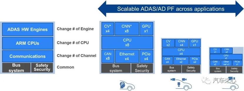
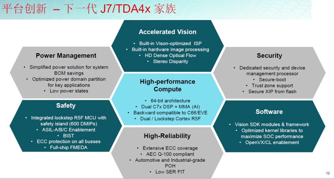
As mentioned earlier, with each increase in the level of autonomous driving, the required computing power of the chips will increase by dozens of times. The computing power requirement for L2 level autonomous driving is only 2-2.5 TOPS, but for L3 level, it requires 20-30 TOPS, and for L4 level, it requires over 200 TOPS, while L5 level requires more than 2000 TOPS.
In the previous chapter, it was noted that Tesla’s computing power is 72 TOPS. The following platforms discussed are all low-computing power platforms below 200 TOPS, mainly for L2 level and above autonomous driving platforms, such as Mobileye, which is primarily strong in vision-based ADAS applications. The low-computing power platform chips include Mobileye, Renesas, TI, and Horizon, which will be introduced one by one in this issue.

Mobileye Solution Introduction
Mobileye was founded in 1999 and is a global pioneer in providing advanced driver assistance systems and autonomous driving solutions based on visual system analysis and data processing in Israel. It provides “chip + algorithm” integrated ADAS visual solutions to 27 OEMs and Tier 1 manufacturers worldwide.
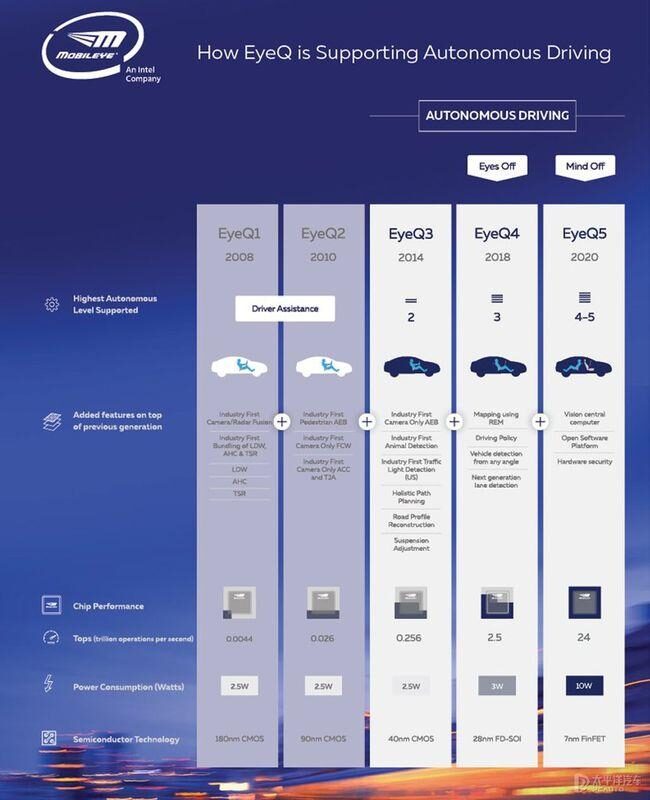
As of the end of 2019, the EyeQ series chips have shipped 54 million units, ensuring driving safety for over 50 million vehicles worldwide, with a current global ADAS market share of about 70%. Since its inception, the company has been committed to providing assistance driving technologies such as pedestrian detection, lane keeping, and adaptive cruise using monocular vision. From 1999 to 2001, Mobileye’s prototype products were iterated annually. In 2001, Mobileye integrated its self-developed algorithms into chips and into vehicles, marking the beginning of the EyeQ chip development.
In April 2004, EyeQ1 began production, and the company subsequently received multiple rounds of financing, shifting its business model to automotive safety, signing cooperation agreements with top global component suppliers such as Continental, STMicroelectronics, Magna, Denso, and Delphi. In 2007, BMW, GM, and Volvo became the first car manufacturers to equip Mobileye chips, and Mobileye products were officially commercialized. In 2008, Mobileye publicly released EyeQ 2, entering a stable development period. By 2013, Mobileye had sold over 1 million products, and subsequent shipments experienced explosive growth. In March 2017, Mobileye was acquired by chip giant Intel for $15.3 billion.
From 2014 to 2019, the company’s revenue compound annual growth rate reached 44%, with 2019 revenue of $879 million and a net profit of 27.9%. The EyeQ series chips shipped 17.4 million units in 2019. Models such as EyeQ1 to EyeQ4 have already been mass-produced, while EyeQ5 is expected to be launched next year. EyeQ4 is mainly used to support semi-automated driving technologies, supporting up to L3 level, while EyeQ5 is primarily positioned for Level 4/5 autonomous driving applications.
By the end of 2019, Mobileye EyeQ chips had cumulatively shipped over 54 million units worldwide.
In September 2020, Mobileye revealed that EyeQ chip shipments had exceeded 60 million units worldwide.
This 60 million includes EyeQ2, EyeQ3, and EyeQ4, with the newly added portion in 2020 mainly being EyeQ4.
Currently, Mobileye has been using an integrated solution of sensor + chip + algorithm, which has led to a decrease in customer development flexibility. In the short term, this is beneficial for increasing market share and is welcomed by OEM manufacturers that are late in transformation or have invested less in AI, but in the long run, it will lead to a lack of ability to customize differentiated products. Therefore, new forces in car manufacturing that need to quickly iterate and upgrade products or OEM manufacturers that require rapid transformation may find it difficult to accept Mobileye’s “black box” approach.
For example, the new force in car manufacturing in China, Xiaopeng Motors, decided to switch from Mobileye’s chips to NVIDIA’s Xavier after briefly testing Mobileye’s chips on the P7, mainly because Xiaopeng wanted to “decouple the chip from the algorithm, use programmable chips, conduct algorithm development and customization on the chips, and combine with scenarios,” thus choosing the more open NVIDIA.
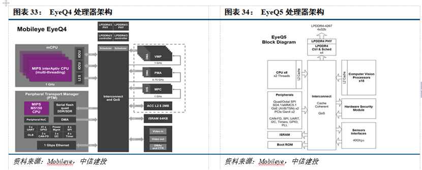
EyeQ4 is equipped with 4 CPU cores and 6 vector microcode processors (VMP), with each CPU core having four hardware threads. The EyeQ4 chip introduces a novel category of accelerators: two multi-threaded processing cluster (MPC) cores and two programmable macro arrays (PMA) cores. Structurally, EyeQ4 uses 28nm FD-SOI. Functionally, compared to EyeQ3, EyeQ4 adds functions such as REM road network collection management, driving decision-making, arbitrary angle vehicle recognition, and drivable area recognition.
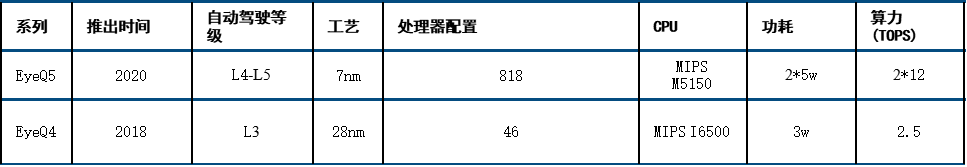
The soon-to-be-launched EyeQ5 will be equipped with 8 multi-threaded CPU cores and will also include 18 next-generation Mobileye visual processors.
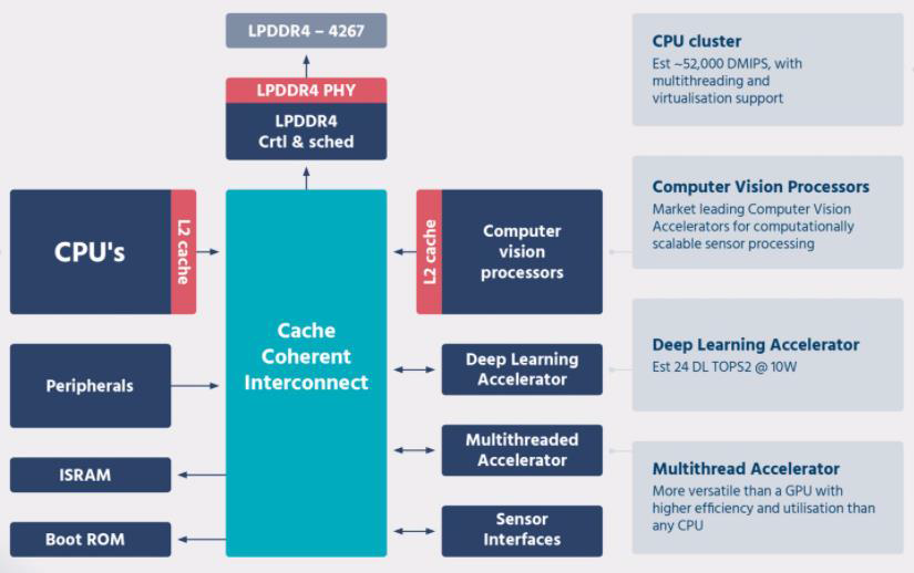
EyeQ5 has more complex functions and will use a 7nm process technology. EyeQ5 supports up to 20 external sensors (cameras, radar, or LiDAR). “Sensor fusion” is the main purpose of EyeQ5. The computing performance of EyeQ5 reaches 12 Tera/second, with energy consumption below 5W, making the chip energy-efficient 2.4 times compared to the benchmark product Drive Xavier. To enable L4/L5 level autonomous driving, Intel’s autonomous driving system will adopt a camera-first design, equipped with two EyeQ5 system chips, one Intel Atom chip, and Mobileye software. EyeQ5 is expected to implement an “open” strategy, allowing Tier 1 and OEM partners to use the “open architecture” to write their own code, including sensor fusion and driving decision-making.
EyeQ5 Mobileye’s SuperVision is about to go into mass production
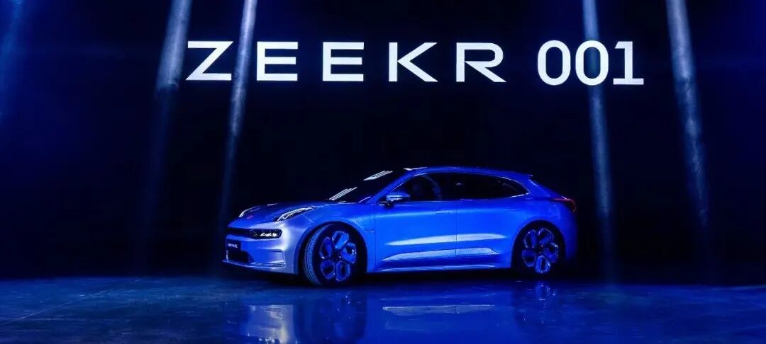
The recently held launch of the Zeekr 001 model uses Mobileye’s SuperVision system for autonomous driving.
SuperVision is a 360° pure vision intelligent driving system built by Mobileye. The so-called pure vision simply means that it uses cameras to achieve L2 and above level assisted driving capabilities, similar to Tesla’s FSD.
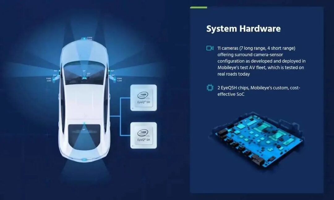
The Zeekr 001 will be equipped with the autonomous driving assistance system Copilot, which integrates 2 Mobileye EyeQ5 chips and the visual perception algorithm SuperVision, making it an L2+ level autonomous driving system.
Two EyeQ5H chips with 24 Tops/10 W will provide computational redundancy for the autonomous driving system. The main system chip will contain the complete technology stack, while the other chip will provide redundant backup to take effect when the main system fails.
The sensor configuration of the Zeekr 001:
-
15 cameras throughout the vehicle;
-
2 high-performance EyeQ5H chips, with EyeQ5 chips built on TSMC’s 7nm FinFET process, achieving a single-chip computing power of 24 Tops, nearly ten times that of EyeQ4;
-
1 250 m LRR long-range millimeter-wave radar;
-
12 ultrasonic radars.
Functional capabilities include:
-
Hands-free high-speed autonomous driving: including automatic lane changing, navigation between different highways, automatic on/off ramps, and urban road assistance;
-
Automatic parking;
-
Standard ADAS functions: including AEB, ACC, and LKA, etc.;
-
DMS driver monitoring system.
Based on this platform, the Zeekr 001 will achieve L2+ level autonomous driving in 2021, similar to the current Tesla’s assisted driving capabilities, while by 2023, it will gradually achieve high-speed NoA or urban NoA.
Mobileye’s Subsequent Product Roadmap
EyeQ5 provides a computing power level of up to 24 TOPS, which is inferior to that of several other competitors.
EyeQ6 is where Mobileye truly focuses on high-performance high-end chips.
EyeQ6 is expected to go into mass production in 2024/2025, with high, medium, and low versions.
Mobileye started designing EyeQ5 in 2016, selecting MIPS’s I6500 as the architecture.
MIPS launched the I6500-F, specifically targeted at automotive applications, based on the I6500 architecture, while the subsequent I7200 is aimed at the wireless market.
As a result, Mobileye decided to abandon the MIPS architecture for the next generation of chips and instead adopt Intel’s Atom core.
Atom is a perennial series in Intel’s processor lineup, with the typical automotive platform being Apollo Lake.
In June 2016, Intel switched from Apollo Lake to the Goldmont architecture and has since been widely used in Tesla, BMW, Cadillac, Hongqi, Hyundai, Volvo, and Chery’s vehicle systems.
EyeQ6 will not go into mass production until 2024, which makes it seem somewhat behind in the competition.

Renesas Autonomous Driving Platform Solution Introduction
Renesas is the second-largest automotive semiconductor manufacturer in the world and the largest automotive MCU manufacturer, as well as the largest semiconductor manufacturer in Japan aside from Sony (whose main business is image sensors).
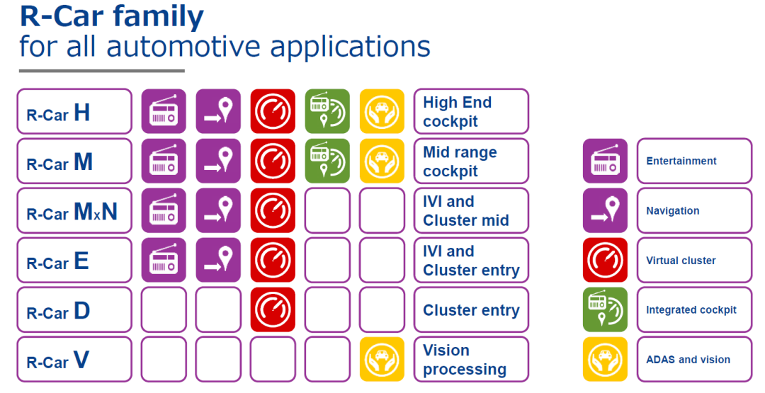
Renesas has layouts in the entire cabin chip (including LCD instrument + central control navigation) and autonomous driving, with different series of products having both entry-level and high-end versions. For example, the middle-level chips in the cabin are the M-level chips, with the M3 series chips used in Volkswagen’s Magotan and Passat, positioned as mid-range cabin chips.
In terms of high-performance automotive computing, Renesas’s top product is the R-CAR H3, mainly used in the cabin field. The latest model of Great Wall’s H6 Lemon platform uses this platform.
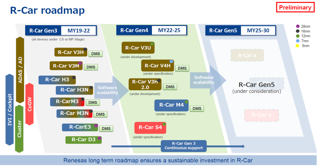
From the roadmap in the above image, it can be seen that Renesas has been relatively slow in launching ADAS chips, with ADAS chips based on the R-Car Gen3 architecture being pushed from 2018 to 2020. R-Car Gen3 is based on the Arm® Cortex®-A57 / A53 cores, which use the Arm 64-bit CPU architecture. It provides the capability to process a large amount of data from multiple sensors around the vehicle. When developing entry-level or high-end systems, there are trade-offs in graphics and computer vision.
The chip launched in 2018 is the R-CAR V3M, which is an SoC mainly used for front camera applications. The challenge faced by front cameras is how to provide high performance for computer vision while supporting low power consumption and a high level of functional safety. Since front cameras are installed close to the windshield, it is necessary to consider the heat generated by the components themselves and the temperature increase caused by direct sunlight. Therefore, the requirements for low power consumption are particularly strict. R-Car V3M solves this problem and improves the efficiency of camera system development.
In 2019, the second visual SoC was launched, namely R-CAR V3H, which has high-performance visual processing capabilities and AI processing capabilities, and boasts industry-leading low power consumption. The target application for this product is the front camera application in L3 and L4 level autonomous driving. The new generation R-Car V3H product has been optimized for stereo front-view applications, improving visual processing performance by 5 times compared to R-Car V3M.
• Four CPU cores: ARM® Cortex®-A53 (1000MHz)
• Supports dual Lockstep ARM Cortex-R7 (800MHz) CPU
• Single-channel 32bit memory controller LPDDR4-3200
• Supports image recognition engine (IMP-X5-V3H)
• Dedicated CNN hardware accelerator, dense optical flow processing, dense stereo vision disparity processing, and object classification algorithms
• Dual image signal processing (ISP)
• Video output (4 lanes × 1 channel LVDS, 1 channel digital)
• Video input (4 lanes × 2 channels MIPI-CSI2, 2 channels digital)
• Supports two CAN-FD interfaces
• One FlexRay interface
• Supports one Gigabit Ethernet and AVB Ethernet
• One PCI Express interface
The AI computing power of this chip is 4 TOPS, and from the computing power and processing speed supported by the chip, it is very suitable for processing image data, making it suitable for front fusion data processing of sensors.
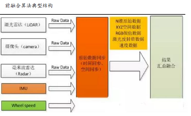
The front fusion algorithm is to fuse the data together at the raw layer, and the fused data is like a super sensor, which has the capability to see infrared, as well as the ability to see camera or RGB, and can also see the three-dimensional data of LiDAR, just like a pair of super eyes. With these super eyes, one can develop their own perception algorithms and finally output a result layer of objects.
Renesas’s V3H aims to create this front fusion super sensor. Bosch’s next-generation vision system incorporates V3H, but due to inherent limitations, it cannot fuse radar data, so Renesas needs to develop an enhanced version of the V3U chip.
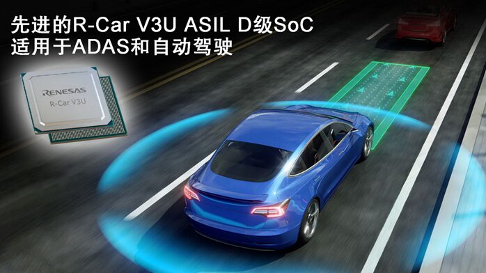
First, it can be seen that V3U is based on the Renesas R-Car Gen 4 architecture, providing scalability from entry-level applications to highly automated driving systems. This component can be used for advanced driver assistance systems (ADAS), allowing the use of air-cooled electronic control units (ECUs), thus bringing advantages in weight and cost.
V3U can simultaneously process data from cameras and radars using a single chip while performing AI-based autonomous driving control and learning, meeting the highest ASIL D requirements of the ISO 26262 automotive safety standard, ensuring system simplicity and safety.
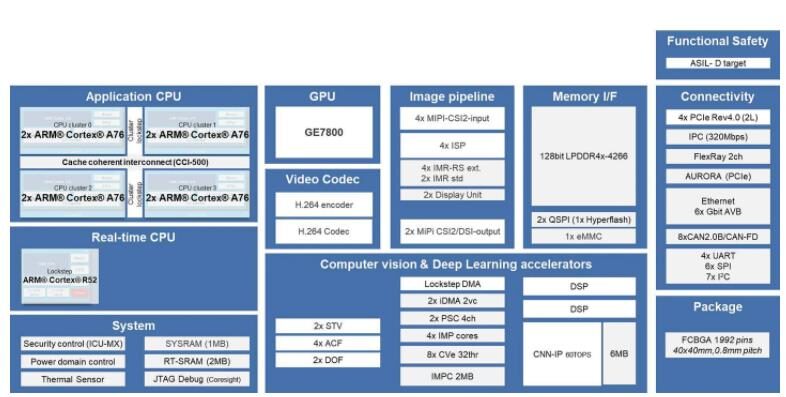
The three major advantages of the R-Car V3U SoC are:
1. High energy efficiency and high-performance convolutional neural network (CNN) hardware accelerator
As the number of sensors used in new-generation ADAS and AD systems continues to increase, the CNN processing performance also needs to be continuously strengthened. By reducing the heat generated by power consumption, air-cooled electronic control units (ECUs) can be installed, thus reducing weight and lowering costs.
Renesas has developed a CNN hardware accelerator core with excellent deep learning performance, and has configured three accelerator cores for R-Car V3U with high density, each CNN accelerator core has 2MB of dedicated memory, totaling 6MB of memory. This reduces data transfer between external DRAM and CNN accelerators by more than 90%.
R-Car V3U also provides various programmable engines, including DSP for radar processing, multi-threaded computer vision engines for traditional computer vision algorithms, image signal processing for enhancing image quality, and other hardware accelerators for key algorithms such as dense optical flow, stereo disparity, and object classification.
Renesas has always excelled in automotive electronics, so low power consumption is its forte, achieving an astonishing energy efficiency of 13.8 TOPS/W, which is six times that of the top EyeQ6, which is very impressive.
R-Car V3U provides highly flexible DNN deep neural network and AI machine learning capabilities. Its flexible architecture can run cutting-edge neural networks for automotive obstacle detection and classification tasks, providing 60.4 TOPS high performance while achieving best-in-class power efficiency of 13.8 TOPS/W.
2. ASIL D system safety mechanism with self-diagnostic capability
The ISO 26262 automotive functional safety standard is a digital target (indicator) for various functional safety levels. The highest functional safety level ASIL D requires a single point failure metric (SPFM) of more than 99% and a latent fault metric (LFM) of more than 90%, thus requiring a very high random hardware fault detection rate. Furthermore, as advanced vehicle operating systems continue to evolve, such as new-generation ADAS and AD systems, the overall functionality of automotive-grade SoCs generally meets ASIL D standards.
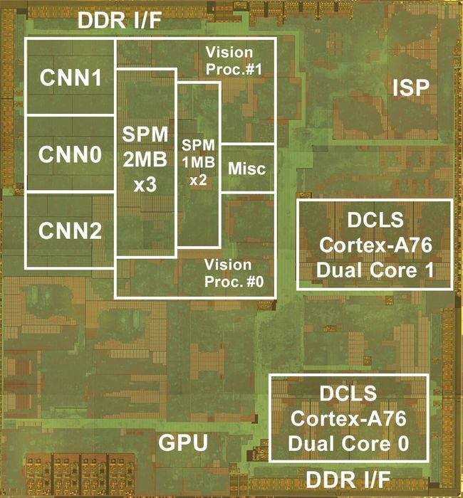
The internal framework of V3U is shown in the above image: it uses an 8-core A76 design. Renesas did not stack 12 A72 cores like Tesla, but instead used ARM’s Corelink CCI-500, which is a Cache Coherent Interconnect. All these redundant chip architecture designs are aimed at meeting ASIL D standards.
Renesas has also developed safety mechanisms for rapid detection and response to random hardware faults occurring in the overall SoC. By combining safety mechanisms suitable for specific target functionalities, it can reduce power consumption while improving fault detection rates. After integrating the above mechanisms into R-Car V3U, most of the signal processing in the SoC can meet ASIL D standards and can have self-diagnostic capabilities, reducing the complexity of fault-tolerant design in AD systems.
3. Support mechanism for keeping software tasks interference-free (FFI)
Keeping software tasks interference-free (FFI) is an important factor in meeting functional safety standards. When there are software components with different safety levels in the system, it is crucial to prevent lower-level tasks from affecting higher-level tasks and causing failures. Additionally, when accessing control registers in hardware modules and shared memory, ensuring FFI in the SoC is also very important. Therefore, Renesas has developed an FFI support mechanism that can monitor all data flowing through the interconnect in the SoC and prevent unauthorized access between tasks. This allows all tasks executed on the SoC to achieve FFI, thus meeting the ASIL D standard application, enabling management of object recognition, integration of sensors with radar/LiDAR, route planning, and issuing control commands through a single chip.
V3U is also a series of products, offering multiple versions to meet the needs of different levels of autonomous driving, aiming to further increase shipments and reduce costs.
The V3U product series adopts a modular design, where A76 can be 2, 4, or 8 cores.
GPUs can also be omitted, and peripherals can be easily added or removed, providing strong flexibility.
Insufficient computing power, safety compensates:
In terms of technology, R-Car V3U is not considered advanced. At least NVIDIA’s next-generation chip series Orin for autonomous driving, announced in May 2020, has CNN computing power ranging from 10 to 2000 TOPS. The chips are produced by TSMC using a 12nm process, and TSMC has begun supplying 5 to 7nm process chips.
When the R-Car V3U samples began shipping on December 17, 2020, the 12nm process technology in the automotive chip field was considered advanced, but Renesas’s scheduled mass production time for R-Car V3U is April to June 2023, which will be somewhat behind.
Among the four major autonomous driving chip manufacturers, namely Mobileye, Renesas, NVIDIA, and Qualcomm, only Renesas’s main business is automotive semiconductors. Although its computing power is slightly behind, it has the deepest understanding of the automotive industry and places the highest importance on vehicle regulations. V3U is the only one among them that can pass ASIL-D, and with the backing of Japanese car manufacturers, Renesas has great hopes.

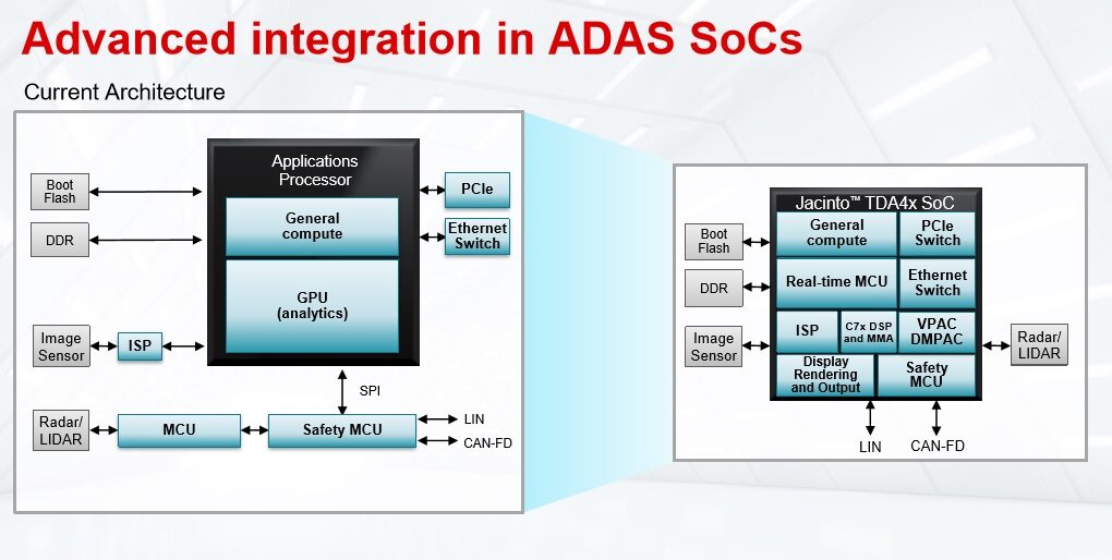
Texas Instruments (TI) Autonomous Driving Platform Solution Introduction
TI chips are traditional automotive chips, along with NXP and Renesas, they are the three major leading manufacturers of traditional cabin chips.
TI actually has two product lines in processors, Jacinto and TDA series.
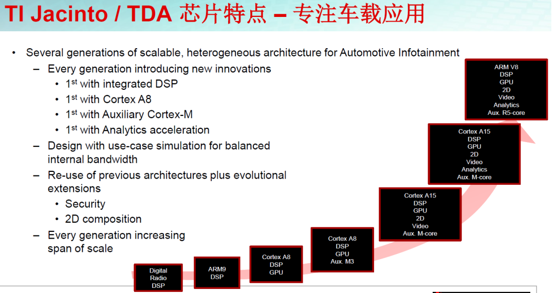
The Jacinto series focuses on digital processors for automotive applications, primarily for in-car infotainment systems.
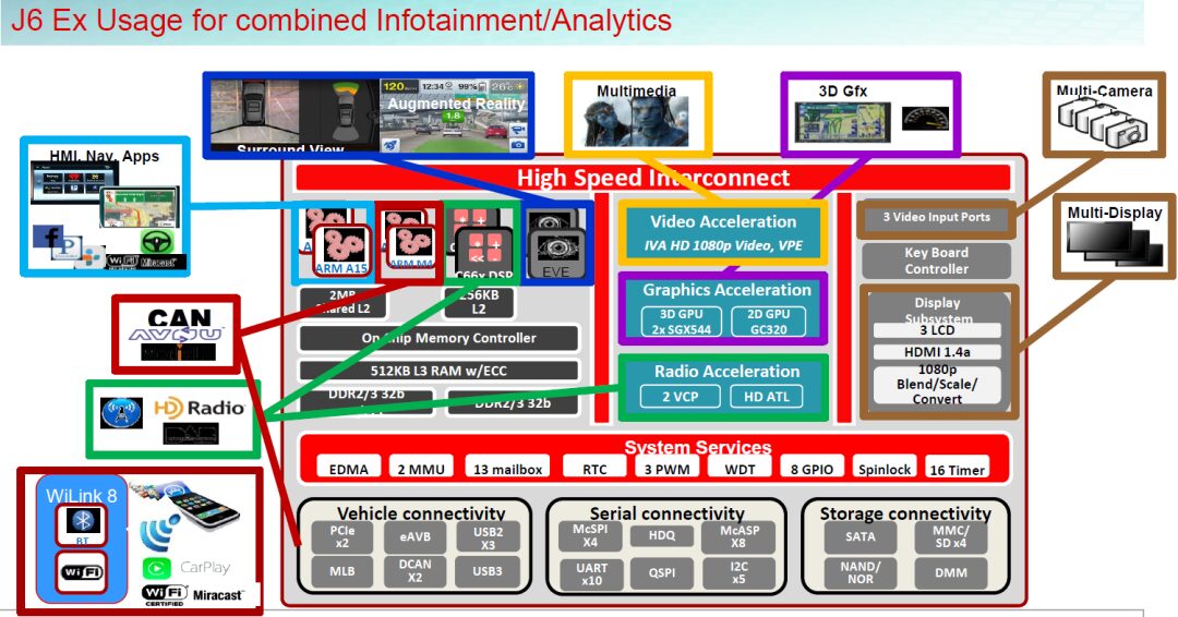
However, from Jacinto6, we can see the combination of in-car infotainment and ADAS functions. This chip includes dual ARM Cortex-A15 cores, two ARM M4 cores, two C66x floating-point DSPs, multiple 3D/2D graphics processors (GPUs from Imagination), and also integrates two EVE accelerators. Whether in processing entertainment media or assisting driving with in-car cameras, it can utilize both internal and external cameras to present various functions such as object and pedestrian detection, enhanced reality navigation, and driver identity recognition.
The TDA series has always focused on ADAS functions, and it can be seen that the TDA series has strong compatibility. The TDA2xV series hardware can perform image processing for surround view, rear view, etc.
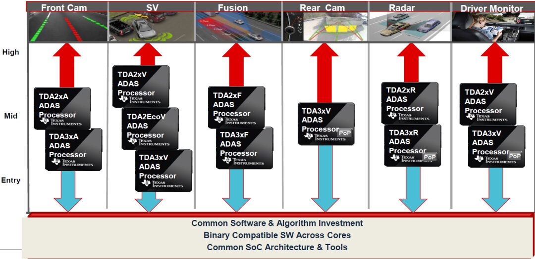
The TDA3x series can support various ADAS algorithms such as lane departure warning, adaptive cruise control, traffic sign recognition, pedestrian and object detection, forward collision warning, and rear collision warning. These algorithms are crucial for effectively utilizing front cameras, all-around views, fusion, radar, and intelligent rear view cameras in many ADAS applications.
The overall hardware and software of the TDA series are backward compatible, with only differences in computing power and applications, making it very convenient for migration.
Autonomous Driving Jacinto 7 Series Architecture Chips
The Jacinto 7 series architecture chips include two automotive-grade chips: the TDA4VM processor and the DRA829V processor, with the former used for ADAS and the latter used for gateway systems, as well as dedicated accelerators for accelerating data-intensive tasks such as computer vision and deep learning. Additionally, these two processors include microcontrollers (MCUs) that support functional safety, enabling automotive manufacturers (OEMs) and Tier 1 suppliers to use a single chip to support ASIL-D high safety requirement tasks and functions.
Many people believe that when the Jacinto 7 platform was released, it basically announced that TI had abandoned the path of cabin domain control chips and shifted towards ADAS and gateway systems, leading many car manufacturers to abandon the selection of TI’s Jacinto 6, as TI will no longer produce cabin domain control chips.
DRA829V Processor Brief Introduction:
Traditional vehicles have generally used low-speed interfaces such as CAN and LIN in the gateway section, but with the evolution of automotive development to domain structures, including power domains, ADAS domains, etc., high-speed bus interfaces are required.
As vehicles become connected, multiple computing resources are needed to manage more data, requiring PCIe and ENET to meet high bandwidth ECU communication both within and between ECUs, while achieving high-level functional safety and supporting network security eHSM.
The DRA829V processor is the industry’s first processor to integrate an on-chip PCIe switch, and it also integrates an Ethernet switch that supports 8-port Gigabit TSN, enabling faster high-performance computing and vehicle-wide communication.
From the above image, it can be seen that the DRA829V is highly integrated, combining traditional safety MCUs, eHSM, and Ethernet switches into a single chip, reducing the complexity of system design. At the same time, it focuses on isolation, ensuring stable performance even when mixing high and low functional levels.
The DRA829V SoC addresses the challenges brought by new vehicle computing architectures by providing computing resources, efficiently moving data within the vehicle computing platform, and enabling communication across the vehicle network, focusing on data interaction and safety.
Many people confuse this chip with the S32G released by NXP. Although both chips are used as gateways, their main starting points are different.

The NXP S32G is designed as a mature network processor to handle tasks such as OTA upgrades for various controllers, data gateway interactions, and transmission of security information, without focusing on forwarding fast signals via PCIe interfaces.
In contrast, the DRA829V focuses more on the collection and forwarding of high-speed signals within the vehicle, while also having gateway control functionality, but gateway control is not the main node, merely an auxiliary function.
TDA4VM Autonomous Driving Chip
Since the vehicles using this chip have not been exposed yet, let’s take a look at the specifications of this chip.
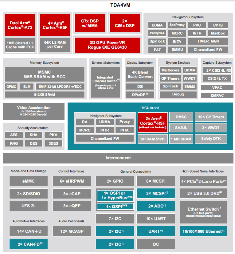
1. Processor cores:
• C7x floating point, vector DSP, up to 1.0 GHz, 80 GFLOPS, 256 GOPS
• Deep-learning matrix multiply accelerator (MMA), up to 8 TOPS (8b) at 1.0 GHz
• Vision Processing Accelerators (VPAC) with Image Signal Processor (ISP) and multiple vision assist accelerators
• Depth and Motion Processing Accelerators (DMPAC)
• Dual 64-bit Arm® Cortex®-A72 microprocessor subsystem at up to 1.8 GHz, 22K DMIPS
– 1MB shared L2 cache per dual-core Cortex®-A72 cluster
– 32KB L1 DCache and 48KB L1 ICache per Cortex®-A72 core
• Six Arm® Cortex®-R5F MCUs at up to 1.0 GHz, 12K DMIPS
– 64K L2 RAM per core memory
– Two Arm® Cortex®-R5F MCUs in isolated MCU subsystem
– Four Arm® Cortex®-R5F MCUs in general compute partition
• Two C66x floating point DSP, up to 1.35 GHz, 40 GFLOPS, 160 GOPS
• 3D GPU PowerVR® Rogue 8XE GE8430, up to 750 MHz, 96 GFLOPS, 6 Gpix/sec
• Custom-designed interconnect fabric supporting near max processing entitlement
Memory subsystem:
• Up to 8MB of on-chip L3 RAM with ECC and coherency
– ECC error protection
– Shared coherent cache
– Supports internal DMA engine
• External Memory Interface (EMIF) module with ECC
– Supports LPDDR4 memory types
– Supports speeds up to 3733 MT/s
– 32-bit data bus with inline ECC up to 14.9GB/s
• General-Purpose Memory Controller (GPMC)
• 512KB on-chip SRAM in MAIN domain, protected by ECC
Safety: targeted to meet ASIL-D for MCU island and ASIL-B for main processor
• Integrated MCU island subsystem of Dual Arm® Cortex®-R5F cores with floating point coprocessor and optional lockstep operation, targeted to meet ASIL-D safety requirements/certification
– 512B Scratchpad RAM memory
– Up to 1MB on-chip RAM with ECC dedicated for R5F
– Integrated Cortex®-R5F MCU island isolated on separate voltage and clock domains
– Dedicated memory and interfaces capable of being isolated from the larger SoC
• The TDA4VM main processor is targeted to meet ASIL-B safety requirements/certification
– Widespread ECC protection of on-chip memory and interconnect
– Built-in self-test (BIST) and
Under normal circumstances, specifications are usually in English; here, I will briefly explain the high-performance parameters.
The TDA4VM processor cores use C7x floating point, vector DSP, up to 1.0 GHz, 80 GFLOPS, 256 GOPS;
The deep learning matrix multiplication accelerator (MMA) can achieve up to 8 TOPS (8b) at 1.0 GHz;
The vision processing accelerator (VPAC) and image signal processor (ISP) and multiple vision assist accelerators;
The depth and motion processing accelerators (DMPAC);
Two 64-bit Arm® Cortex®-A72 microprocessor subsystems can operate at up to 1.8 GHz, with 22K DMIPS;
Each Cortex®-A72 core integrates 32KB L1 DCache and 48KB L1 ICache, with six Arm® Cortex®-R5F MCUs operating at up to 1.0 GHz, with 12K DMIPS;
Each core has 64K L2 RAM, with two Arm® Cortex®-R5F MCUs in an isolated MCU subsystem, and four Arm® Cortex®-R5F MCUs in a general compute partition, and two C66x floating point DSPs operating at up to 1.35 GHz, with 40 GFLOPS, 160 GOPS;
The TDA4VM processor consumes only 5 to 20W of power to perform high-performance ADAS calculations without the need for active cooling.
High-performance core overview:
The “C7x” next-generation DSP integrates TI’s industry-leading DSP and EVE cores into a single, higher-performance core while adding floating-point vector computation capabilities, ensuring backward compatibility with old code while simplifying software programming. In typical automotive worst-case temperature conditions of 125°C, the new “MMA” deep learning accelerator can achieve up to 8 TOPS of performance within the industry’s lowest power envelope. Dedicated ADAS/AV hardware accelerators can provide visual preprocessing as well as distance and motion processing without compromising system performance.
TI’s TDA4VM processor series is based on the Jacinto™ 7 architecture, targeting driving assistance systems (ADAS) and autonomous vehicles (AV). The TDA4VM processor has powerful on-chip data analysis capabilities and, when combined with vision preprocessing accelerators, makes system performance more efficient. Automotive manufacturers and Tier 1 suppliers can use it to develop front camera applications using high-resolution 8-megapixel cameras, helping vehicles see farther and incorporate more driving assistance enhancements.
Moreover, the TDA4VM processor can simultaneously operate 4 to 6 3-megapixel cameras while also fusing data from other sensors such as radar, LiDAR, and ultrasound onto a single chip. This multi-level processing capability enables the TDA4VM to serve as the centralized processing unit for ADAS, thus realizing key functionalities in autonomous parking applications (such as surround view and image rendering display), while enhancing the vehicle’s perception capabilities to achieve 360-degree recognition.
From the overall chip performance and functionality perspective, combined with the autonomous driving system architecture, TI’s ADAS chips and Renesas’s V3H are very similar, both focusing on image or radar data fusion processing, and both emphasizing low power consumption, requiring very powerful algorithms to enhance the chip’s processing capabilities, ultimately feeding the processed signals back to the control chip.
TDA4M Advantages:
Improving vehicle perception capabilities with lower power consumption
By integrating camera, radar, and LiDAR data, ADAS technology helps cars see and adapt to the surrounding world. A large influx of information into the vehicle means that the processor or system-on-chip needs to quickly and effectively manage multi-level data processing in real-time while meeting system power consumption requirements. TI’s new processor performs high-performance ADAS calculations using only 5 to 20W of power, without the need for active cooling.
TDA4VM provides high-performance computing for traditional and deep learning algorithms with industry-leading power/performance ratios, and has a high level of system integration, thus enabling scalability and lower costs for advanced automotive platforms supporting centralized ECUs or multiple sensor modes from independent sensors.
Key cores include next-generation DSPs with scalar and vector cores, dedicated deep learning and traditional algorithm accelerators, the latest Arm and GPU processors for general computing, integrated next-generation imaging subsystems (ISP), video codecs, Ethernet hubs, and isolated MCU islands, all of which are protected by automotive-grade safety hardware accelerators.

Horizon Autonomous Driving Platform Solution Introduction
Horizon possesses leading AI algorithms and chip design capabilities, developing high-performance, low-cost, and low-power edge AI chips and solutions through a combination of software and hardware, focusing on intelligent driving and AIoT. Horizon can provide ultra-high cost-performance edge AI chips, exceptional power efficiency, an open toolchain, rich algorithm model examples, and comprehensive empowerment services.
Relying on industry-leading software and hardware products, Horizon provides customers with a complete solution of “chip + algorithm + toolchain”. In the intelligent driving field, Horizon’s business ties with the four major automotive markets (the US, Germany, Japan, and China) continue to deepen, and it has empowered partners including Audi, Bosch, Changan, BYD, SAIC, GAC, and other top Tier 1s and OEM manufacturers.
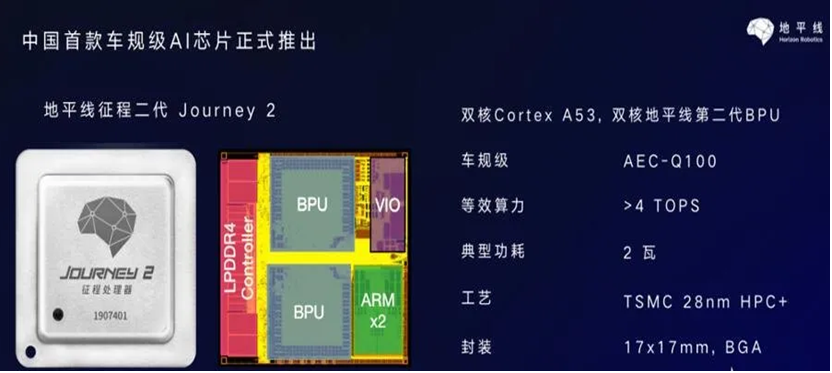
In the AIoT field, Horizon has partnered with national-level development zones, leading manufacturing enterprises, modern shopping centers, and well-known brand stores. Currently, based on the innovative AI-specific computing architecture BPU (Brain Processing Unit), Horizon has successfully mass-produced China’s first edge AI processor focused on intelligent driving – the “Journey” series processor and the “Sunrise” series processor focused on AIoT, which have been commercially deployed on a large scale.
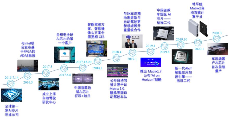
On the road to automotive-grade chips, the company has strong patience and long-term strategic capabilities. The launch of Changan UNI-T in June 2020 marked the Journey II becoming China’s first mass-produced AI chip for vehicles. The long march has made significant progress. Compared with other AI chip newcomers who entered consumer-level scenarios such as mobile phones and cameras at the outset to quickly achieve revenue growth, Horizon has chosen the most challenging path, taking on the Everest of the AI industry – automotive-grade AI chips, and entering the arena to compete with traditional chip giants.
Since its establishment in 2015, Horizon has achieved mass production of automotive-grade AI chips in just five years, marking the beginning of the first year of mass production of domestic automotive-grade AI chips. The company currently has multiple orders for designated projects from OEMs, and it is expected to see explosive revenue and performance growth from 2020 to 2023. Considering the time required for sample production, automotive-grade certification, and model introduction, achieving mass production of automotive-grade AI chips within five years of establishment places Horizon at a leading position in the automotive electronics industry. In contrast, Mobileye’s automotive-grade chips took 8 years from development to official commercialization; as the global leader in general-purpose AI chips, NVIDIA took 9 years after the release of CUDA to apply the K1 chip to Audi A8’s vehicle system.
The Journey series chips can simultaneously support intelligent cockpit AI applications and autonomous driving applications, applied in both intelligent cockpit and autonomous driving domains, ultimately becoming the main control chip for centralized computing platforms. Currently, the second generation of Journey can support L2 autonomous driving applications, while the next generation of chips will support L3/L4 autonomous driving applications.
The future intelligent cockpit will upgrade interaction methods, such as in-car vision (optical), voice (acoustic), and chassis and body data such as steering wheel, brake pedal, accelerator pedal, gear lever, and seatbelt, using biometric technology (mainly facial recognition and voice recognition in the cabin) to comprehensively assess the physiological state (such as appearance, facial features, etc.) and behavioral state (such as driving behavior, voice, physical behavior) of the driver (or other passengers), making the vehicle truly “understand” humans and transforming the cockpit into a comprehensive “personal assistant”.
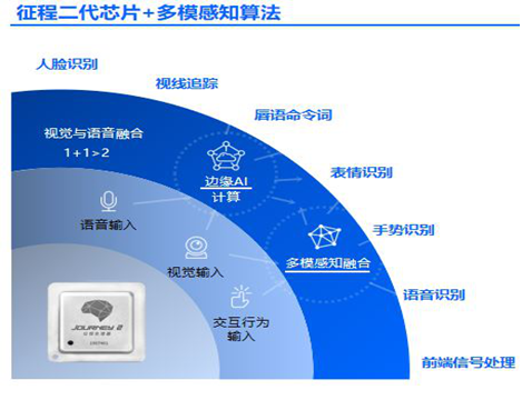
Therefore, the second-generation Journey chip released last year has strong support capabilities for multi-modal perception algorithms in intelligent cockpits, and was officially commercialized on Changan’s SUV model UNI-T launched in April 2020. Currently, the intelligent cockpit functions of UNI-T, such as gaze-based screen activation, distraction reminders, fatigue monitoring, and intelligent voice photo-taking, have all reached mature and stable high standards of user experience.
Currently, the second-generation Journey can perform real-time detection and accurate recognition of multiple targets, providing high-precision and low-latency perception outputs to meet the needs of intelligent driving scenarios such as visual perception, visual mapping, positioning, visual ADAS, and the functional requirements of intelligent human-computer interaction such as voice recognition, eye tracking, and gesture recognition.
It can run more than 60 classification tasks simultaneously, with the number of targets recognized per second exceeding 2000, thus fully meeting the visual application needs of L2 level intelligent driving. It is expected that from 2020 to 2021, we will see mass-produced vehicles equipped with the Journey series chips achieving ADAS functionality.
In January 2020, Horizon announced the launch of its next-generation autonomous driving computing platform – Matrix 2.0, equipped with Horizon’s second-generation automotive-grade chip, capable of meeting L2 to L4 level autonomous driving demands. In terms of perception, Matrix 2.0 can support multi-sensor perception and fusion, including cameras and LiDAR, achieving up to 23 categories of semantic segmentation and six major categories of object detection. The perception algorithm can also cope with complex environments, supporting stable perception results even in special scenarios or extreme weather conditions.

In the Robotaxi field, Horizon has reached cooperation with several top autonomous driving operation companies. Currently, Matrix is applied to nearly a thousand test vehicles and has already commenced commercial operation services. In the OEM field, Horizon has long-term collaborations with Audi in the R&D and productization of high-level autonomous driving technology, assisting Audi in obtaining an L4 road test license in Wuxi. Audi China was also the first to demonstrate passenger vehicle platooning L4 autonomous driving and vehicle-road collaboration in domestic highways using the Matrix computing platform.
The new product roadmap is clear, and the next-generation chips are in the research and development and actual tape-out stages, with expectations that single-chip computing power will approach 100 TOPS in the future, processing up to 16 video signals. The successful commercialization of the second-generation Journey chip marks a new milestone for the company. Currently, the second-generation Journey has received multiple pre-installed orders from market customers in various countries. The subsequent upgrades and planning of the company’s new products are also rapidly advancing and landing, with excellent commercial achievements stemming from continuous forward-looking technological exploration and rapid iteration of AI chip products.
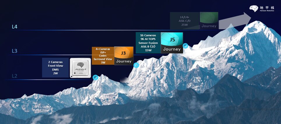
As a global leader in edge AI chips, Horizon successfully launched the automotive-grade AI chip Journey 2 in 2019, and this year will launch the flagship chip Journey 5 aimed at high-level autonomous driving, with AI computing power reaching 96 TOPS, actual performance leading internationally, and will provide extreme efficiency and comprehensive flexible empowerment services for the industry’s practical needs based on edge AI chips.

On May 9, it was reported that the domestic automotive AI chip manufacturer Horizon officially announced that its third-generation automotive-grade product, aimed at L4 high-level autonomous driving with high computing power, the Journey 5 series chip, has successfully completed tape-out ahead of schedule and successfully powered on!
—END—