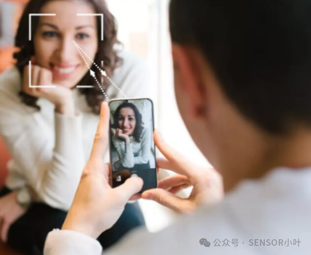
From automatic sensing faucets to AR/VR headsets, robots, and autonomous vehicles—products that can “see” the surrounding world like humans are becoming ubiquitous. To create products that can “see” the world, camera sensors are the preferred technology. However, the real world is three-dimensional, while a standalone camera can only capture 2D images. To be effective, they also need to obtain depth information. For example: automatic sensing faucets need to recognize the distance to a hand, robots and autonomous vehicles need to detect the distance to objects to avoid collisions, and augmented reality experiences require a 3D map of real-world scenes.
Depth sensing technology can directly measure the distance between the sensor and surrounding objects. When necessary, it can be combined with 2D image data using techniques such as Simultaneous Localization and Mapping (SLAM) to create a complete 3D map of the scene, obtaining the six degrees of freedom position within the scene.
Depth sensors are special sensors primarily used to measure and perceive the depth information of objects or scenes in three-dimensional space, known as depth perception. Depth sensors can acquire distance information in three-dimensional space through specific technical means. This distance information is usually presented in the form of a depth map, which is a collection of all three-dimensional points in a scene, with each point representing a specific location of an object or scene, along with corresponding depth information.
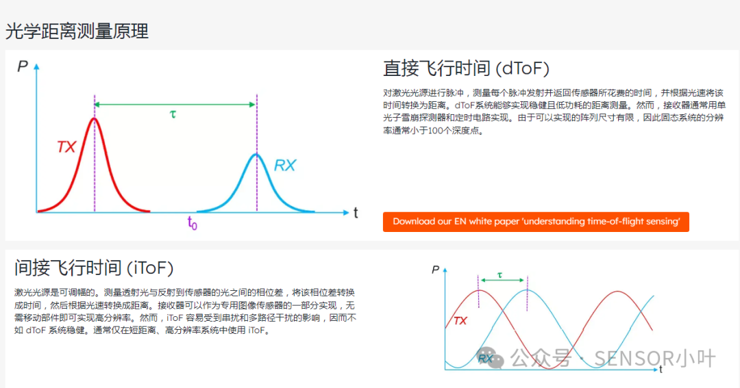
The working principles of depth sensors vary, but they mainly calculate distance based on parameters such as the time or phase difference of light reflecting off the surface of an object back to the sensor. For example, the Time-of-Flight (ToF) sensor is a common depth sensor that actively emits modulated light to the target surface and then observes and calculates the corresponding reflected light. The phase difference between the emitted and reflected light is computed to obtain the distance/depth..
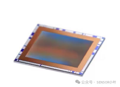 VD55H1 is a low-noise, low-power 672 x 804 pixel (0.54 megapixel) indirect Time-of-Flight (iToF) sensor chip manufactured using advanced back-illuminated stacked wafer technology. Combined with a 940 nm illumination system, it can construct a compact 3D camera, producing high-definition depth maps with typical ranging distances of up to 5 m at full resolution, and can exceed 5 m using patterned illumination. With its unique ability to operate at a modulation frequency of 200 MHz and over 85% demodulation contrast, the depth accuracy produced by this sensor is twice that of typical 100 MHz modulation sensors, while multi-frequency operation provides long-range ranging capabilities. The low-power 4.6 µm pixel achieves advanced power performance, with average sensor power consumption dropping below 80 mW in certain modes.
VD55H1 outputs 12-bit RAW digital video data at 1.5 GHz via MIPI CSI-2 four-channel or dual-channel interfaces. The sensor frame rate can reach up to 60 fps at full resolution and up to 120 fps in analog merged 2×2 mode. STMicroelectronics has developed proprietary software image signal processing (ISP) to convert RAW data into depth maps, amplitude maps, confidence maps, and offset maps. It also supports Android formats such as DEPTH16 and depth point clouds. The device can be fully configured via an I2C serial interface. It features 200 MHz low-voltage differential signaling (LVDS) and 10 MHz, 3-wire SPI interfaces for highly flexible control of the laser driver. The sensor is optimized for low electromagnetic interference/electromagnetic compatibility, multi-device immunity, and easy calibration procedures.
VD55H1 is a low-noise, low-power 672 x 804 pixel (0.54 megapixel) indirect Time-of-Flight (iToF) sensor chip manufactured using advanced back-illuminated stacked wafer technology. Combined with a 940 nm illumination system, it can construct a compact 3D camera, producing high-definition depth maps with typical ranging distances of up to 5 m at full resolution, and can exceed 5 m using patterned illumination. With its unique ability to operate at a modulation frequency of 200 MHz and over 85% demodulation contrast, the depth accuracy produced by this sensor is twice that of typical 100 MHz modulation sensors, while multi-frequency operation provides long-range ranging capabilities. The low-power 4.6 µm pixel achieves advanced power performance, with average sensor power consumption dropping below 80 mW in certain modes.
VD55H1 outputs 12-bit RAW digital video data at 1.5 GHz via MIPI CSI-2 four-channel or dual-channel interfaces. The sensor frame rate can reach up to 60 fps at full resolution and up to 120 fps in analog merged 2×2 mode. STMicroelectronics has developed proprietary software image signal processing (ISP) to convert RAW data into depth maps, amplitude maps, confidence maps, and offset maps. It also supports Android formats such as DEPTH16 and depth point clouds. The device can be fully configured via an I2C serial interface. It features 200 MHz low-voltage differential signaling (LVDS) and 10 MHz, 3-wire SPI interfaces for highly flexible control of the laser driver. The sensor is optimized for low electromagnetic interference/electromagnetic compatibility, multi-device immunity, and easy calibration procedures.
 Ultra-compact 0.54 megapixel iToF sensor chip
-
672 x 804 indirect Time-of-Flight (iToF) sensor chip (0.54 megapixel)
-
4.6 μm back-illuminated fast photodiode pixels, 1/4 inch optical format
-
4.5 mm x 4.9 mm chip manufactured using advanced 40 nm stacked wafer technology
Achieving low-power, high-precision depth maps
-
Pixels have over 85% demodulation contrast at a modulation frequency of 200 MHz
-
Low-noise charge domain pixels (no kTC) below 5e-
-
Supports multi-frequency (up to three frequencies)
-
Average sensor power consumption drops to 80 mW
-
Smart iToF modulation, no swing error calibration required
-
Multi-user interference reduction
-
Optimized for low electromagnetic interference/compatibility
Easy integration of 3D cameras
Outputs raw data at 1.5 GHz on MIPI CSI2 interface (four-channel or dual-channel)
10/12 bit configurable ADC resolution
Sensor raw output up to 120 fps (depth level frame rate)
Sensor control: fast mode + I2C slave interface (up to 1 MHz)
Laser driver interface: LVDS and 3-wire SPI
Provides software ISP for depth reconstruction