1. Why Change the Approach to Learning FPGA?
Hello everyone, I am Du Yong, a senior FPGA digital signal processing algorithm engineer, a university teacher, and a content creator. In my spare time, I enjoy watching sports, movies, listening to music, reading, and jogging. I feel that a happy life is one where I can watch sports, drink tea, and wait for the FPGA program to run its results.
After years of FPGA project design, I have reflected on the helplessness I felt when I was learning the relevant technology due to the lack of usable reference materials (mainly the lack of practical engineering implementation materials). With a small hope of reducing the confusion for future learners, I coincidentally had a relatively long period of free time, so I started writing a series of books on digital signal processing, such as “MATLAB and FPGA Implementation of Digital Filters”. Looking back, it has already been 11 years since 2012. I have since published books on communication synchronization, modulation and demodulation, phase-locked loop technology, digital signal processing design, and more on FPGA design and implementation.
I am fortunate to have been engaged in FPGA design-related work for over twenty years and have personally felt the rapid development of FPGA technology.
However, many people say that it is difficult to get started!
Currently, many universities have started offering FPGA courses from the undergraduate level, and more and more schools are beginning to integrate traditional “Digital Circuit Technology” courses with FPGA technology courses. Although the entry barrier for FPGA technology is high, its development trend is irreversible. In some classrooms, while carefully explaining the complex syntax of Verilog HDL, students are reassured because the syntax is somewhat similar to C language, easing their fear of hardware description languages.
In digital circuit technology, combinational logic is straightforward and easy to grasp, but students struggle with the subsequent sequential logic design, especially the analysis and understanding of state equations. Solving equations? This is quite similar to mathematical problems! However, the real challenge lies ahead, where one must use a state machine to describe a sequential logic circuit that is not very familiar. Teacher, how many states should this functional circuit be divided into? How do I draw a state transition diagram? After experiencing a brief and enjoyable design of combinational logic circuits, students soon encounter the relentless obstacles of sequential logic design.
When using Verilog HDL language, describing hardware circuits with the well-trained mindset of C language leads to confusion once again. What is the difference between “=” and “<=”? Why is it called blocking assignment? Why is it called non-blocking assignment? What is immediate execution, and what is sequential execution? When are “=” and “<=” the same, and when are they different? Why can C language be written this way, but Verilog HDL cannot?
Perhaps, we can change our approach to learning FPGA!
We need to understand that Verilog HDL is essentially a parallel language, while C language is a sequential language. Apart from their similar appearance, they are fundamentally different! Once we understand the timing waveforms of D flip-flops, using a parallel language mindset to comprehend “=” and “<=” will make everything clear and enlightening.
Timing essentially refers to the order of events over time. Driven by the clock, counting can generate various time-related signals. Designing sequential logic is essentially designing counters. Who cannot master counters?
Perhaps, we can change our approach to learning FPGA!
Temporarily set aside the concept of state machines and the obsession with sequential language thinking. Following the working methods of digital circuits, we start with D flip-flops and counters to elaborate on the essence of parallel language, breaking through the learning barriers of hardware description languages and stepping into the world of FPGA technology.
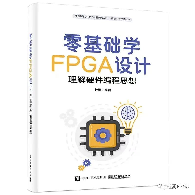
“Learn FPGA From Scratch: Understanding Hardware Programming Ideas” is a book I published in April 2023 through the Electronics Industry Press, specifically written for FPGA beginners, hoping to help everyone quickly cross the threshold of FPGA technology.
2. Why Use Domestic FPGA?
In recent years, the chip industry, both internationally and domestically, is undergoing significant changes. AMD and Intel still dominate the global FPGA market, but have you ever experienced the difficulty of not being able to purchase chips? Or faced the situation where the price from suppliers was too high to afford when you wanted to mass-produce a well-designed development board?
More importantly, perhaps it is due to a fierce operation from the US, the rise of domestic chips is an unstoppable trend. As someone who has been engaged in FPGA design for a long time, I have clearly noticed a rapid increase in projects developed using domestic FPGA in recent years.
Coincidentally, I had the opportunity to collaborate with Gao Yun FPGA to launch an entry-level book on domestic FPGA development platforms.
To be honest, Gao Yun’s Cloud Source software and other domestic FPGA development software still have significant gaps compared to ISE, Vivado, and Quartus, but this mainly reflects in advanced applications. For beginners, however, the domestic FPGA development environment is much more user-friendly. From the installation process to the usage steps, it is more approachable, allowing beginners to spend less time learning the complex usage of development tools. The core of learning FPGA is to understand hardware programming concepts and master hardware programming methods. The usage of development environments is largely similar. Trust me, and trust the firsthand experiences of thousands of FPGA development engineers. Once you are familiar with FPGA development methods, learning other development environments will definitely be a pleasant and easy task. Just as if you master Verilog HDL language, even if you have never written VHDL code, the first time you see a piece of VHDL code, you will feel an incredible familiarity because they are not fundamentally different.
3. Are the Videos Complete? Are They Recorded Seriously? Are They Completely Free?
Yes, they are complete, recorded seriously, and completely free.
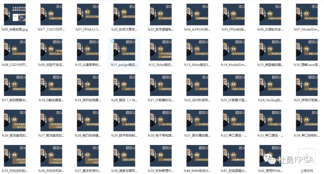
I completed the recording of 42 accompanying videos from the end of 2022 to early 2023, which have been published on Bilibili (Content Creator: Du Yong FPGA). While watching the videos, you may notice that some episodes have a slightly hoarse voice, as if I had a cold? Perhaps you have already guessed. I was fortunate to experience a baptism during the global pandemic.
Spring has returned, and all things are revived. The crowds during the May Day holiday make that pandemic feel like a distant memory!
4. Reason for Chapter Arrangement
The book is divided into four parts: Basic Part, Introduction Part, Entry Part, and Improvement Part.
The Basic Part only introduces the core content related to FPGA design from the digital circuit course in one chapter. The next two chapters discuss the basics of logic circuits and the environment installation methods.
The Introduction Part starts with the LED flowing light circuit to experience the FPGA development process. You will find it is much simpler than you imagined, especially when using Cloud Source software. We elaborate on the soul of D flip-flops and the essence of counters from multiple angles. Have we talked too much about these two simple contents? No, no, no. Based on the idea of “changing the approach,” writing FPGA programs is merely repeatedly writing D flip-flops and counters, regardless of whether it is the stopwatch circuit, serial port circuit, or music player, it is all the same. When discussing D flip-flops and counters, we emphasize integrating the FPGA parallel design philosophy, clearly and thoroughly understanding concepts like “=” and “<=” which are fundamentally different from C language.
The Entry Part begins to take off. The stopwatch circuit is designed by almost everyone, and there are many learning codes available online. What kind of code is concise and beautiful? If you find code similar to what is in this book, and if the code was published before 2019 (I released basic codes like stopwatch, button debounce, serial communication in 2019), it can only be said that the aesthetics of the publisher and I are quite similar. If all of them were published after 2019, I hope everyone can indicate the source when using them. The design problems of password locks and electronic piano circuits have initially exceeded the scope of FPGA syntax; they are merely training learners’ logical thinking abilities. Serial communication is a widely used functional circuit. I often see students finding serial port codes written using state machines online. Why use state machines? Using counters is much simpler and clearer from both understanding and implementation perspectives. Although I do not advocate writing code with a state machine mindset, I still dedicated a chapter to discuss it and provided a comparative analysis using the sequential detector program as an example. Writing a sequential detector using the idea of D flip-flops is incredibly simple!
The Improvement Part discusses timing constraints, IP core design, online logic analyzers, and common design techniques. After experiencing the learning from the first three parts, if beginners can write a complete “serial control stopwatch circuit” from scratch without referencing any code, they have basically crossed the threshold of FPGA design and possess the conditions and abilities to self-learn this part.
5. Learning is Endless
No book can cover every aspect of FPGA design. Mastering all techniques of FPGA design through one book is merely a beautiful wish. Proficient application requires a lot of practice and thinking from learners. “Learn FPGA From Scratch: Understanding Hardware Programming Ideas” merely adopts another approach to provide everyone with a different learning method, helping them quickly and smoothly enter the world of FPGA design.
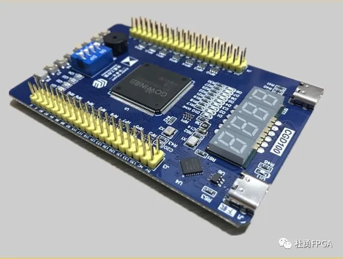
Do you have to have the CGD100 development board, and must you use Cloud Source software to use this book? No, no, no.
The important thing is said three times: the development environment is secondary; the core is to understand hardware programming concepts, concepts, concepts!
6. Book Directory
Chapter 1: Essential Digital Logic Circuit Knowledge
Chapter 2: Basics of Programmable Logic Devices
Chapter 3: Preparing the Design Environment
Part Two: Introduction Part
Chapter 4: FPGA Design Process—LED Flowing Light Circuit
Chapter 5: Starting from Combinational Logic Circuits
5.1 Starting from the Simplest NAND Gate Circuit
5.1.1 Calling Gate-Level Structure to Describe NAND Gate
5.1.2 Naming Principles of Two-in-One
5.1.3 Building a Voting Circuit with Gate-Level Circuits
5.2 Designing a More Complex Voting Circuit
5.2.1 Shortcomings of Gate Circuit Design Methods
5.2.2 Completing Gate Circuit Function with Assign Statement
5.2.3 The Most Common If-Else Statement
5.2.4 Differences Between Reg and Wire Usage
5.2.5 Remembering the Rules of “<=” and “=” Assignments
5.2.6 Very Important Concept—Signal Bit Width
5.2.7 Behavioral Modeling of a 5-Person Voting Circuit
5.3 ModelSim Simulation of Circuit Function
5.3.1 4-Line to 2-Line Encoder Design
5.3.2 Establishing a ModelSim Project
5.3.3 Designing Test Stimulus Files
5.3.4 Viewing ModelSim Simulation Waveforms
5.4 Typical Combinational Logic Circuit Verilog HDL Design
5.4.1 8421 BCD Encoder Circuit
5.4.2 8-Line to 3-Line Priority Encoder Circuit
5.4.3 74LS138 Decoder Circuit
5.4.4 Case Statement Equally Famous as If-Else
5.4.5 Data Distributors and Selectors Circuit
5.5 Static Display Circuit Design for Digital Tubes
5.5.1 Basic Working Principle of Digital Tubes
5.5.2 Instance Requirements and Circuit Principle Analysis
5.5.3 Verilog HDL Design of Digital Tube Display Circuit
5.5.4 On-Board Testing
Chapter 6: The Soul of Sequential Logic Circuits—D Flip-Flops
6.1 In-Depth Understanding of D Flip-Flops
6.1.1 D Flip-Flops Produce a One Clock Cycle Delay
6.1.2 The Maximum Clock Frequency at Which D Flip-Flops Can Operate
6.2 Description Methods of D Flip-Flops
6.2.1 Verilog HDL Design of a Single Flip-Flop
6.2.2 D Flip-Flops with Asynchronous Reset Signal
6.2.3 D Flip-Flops with Synchronous Reset Signal
6.2.4 D Flip-Flops with Clock Enable Signal
6.2.5 ModelSim Simulation of D Flip-Flops
6.2.6 Other Forms of D Flip-Flops
6.3 First Trial—Edge Detection Circuit Design
6.3.1 Function Description of Edge Detection
6.3.2 Verilog HDL Design of Edge Detection Circuit
6.3.3 Improved Edge Detection Circuit
6.4 Continuous Sequence Detector—Upgrade of Edge Detection Circuit
6.4.1 Continuous Sequence Detection Circuit Design
6.4.2 Analyzing Verilog HDL Parallel Statements
6.4.3 Re-discussing “<=” and “=” Assignments
6.4.4 ModelSim Simulation of the Sequence Detector
6.5 Arbitrary Sequence Detector—Feeling the Power of D Flip-Flops
6.5.1 Completing the Design Function of Beverage Weight Detection Circuit
6.5.2 Optimizing the Design Code of Detection Circuit
Chapter 7: The Essence of Sequential Logic Circuits—Counters
7.1 Simple 16-Bit Counter
7.1.1 Completing Counter Design with Two Lines of Code
7.1.2 A Counter is Just an Adder and a Flip-Flop
7.2 Decimal Counter
7.2.1 Counter with Reset and Clock Enable Signals
7.2.2 Discussing the Base of Counters
7.2.3 Various Writing Methods for Counters
7.3 Counters are the Core of Flowing Lights
7.3.1 Designing a Second Signal
7.3.2 Design Plan for Flowing Light Circuit
7.3.3 Flowing Light with Controllable Flashing Frequency
7.3.4 Designing Flowing Light Circuit Using Shift Operations
7.4 The Essence of Verilog is Parallel Language
7.4.1 Typical Verilog Error—Repeated Assignment to the Same Signal
7.4.2 Parallel Language vs. Sequential Language
7.4.3 Analyzing Signal Repeated Assignment Issues with Parallel Thinking
7.5 Breathing Light Circuit Design
7.5.1 Working Principle of Breathing Light
7.5.2 Design Thought Analysis
7.5.3 Brightness Implementation Module Verilog Design
7.5.4 Brightness Control Module Verilog Design
7.5.5 Top-Level Module Verilog Design
Part Three: Entry Part
Chapter 8: Designing a Concise and Beautiful Stopwatch Circuit
8.1.1 Setting a Goal—4-Digit Stopwatch Function
8.1.2 Clarifying Functional Requirements
8.1.3 Formulating a Design Plan
8.2 Verilog Design of Top-Level Files
8.3 Designing a Complete Digital Tube Display Module
8.4 Verilog Design of Stopwatch Counting Module
8.4.1 One-Step Stopwatch Counting Circuit Design
8.4.2 ModelSim Simulation of Stopwatch Counting Circuit
8.4.3 Concise and Beautiful Stopwatch Timer Design
8.4.4 Implementing Start/Stop Functions for Stopwatch
8.5 Verilog Design of Button Debounce Module
8.4.5 Principles of Button Debounce Generation
8.4.6 Debounce Circuit Verilog Design
8.4.7 Integrating Debounce Module into Stopwatch Counter
Chapter 9: Digital Password Lock Circuit Design
9.1 Function Description of Password Lock
9.2 Planning the Functional Modules of Password Lock
9.2.1 Overall Structure Block Diagram of Password Lock
9.2.2 Top-Level Module Design of Password Lock
9.3 Functional Sub-Module Design of Password Lock
9.3.1 Verilog Design of Button Debounce Module
9.3.2 Verilog Design of Counting Module
9.3.3 Password Setting Module is the Core Module
Chapter 10: Simple Electronic Piano Circuit Design
10.1 Principle of Note Generation
10.2 Key Function Circuit Design
10.2.1 Top-Level Module Design
10.2.2 Key Module Design
10.2.3 Note Generation Module Design
10.3 Automatically Playing the Piece “Liang Zhu”
10.3.1 Principle of Automatically Playing the Piece
10.3.2 Automatically Playing the Segment of “Liang Zhu”
10.4 Complete Electronic Piano Circuit Design
Chapter 11: Widely Used Serial Communication Circuit
11.1 Concept of RS-232 Serial Communication
11.2 Analysis of Serial Port Hardware Circuit Principles
11.3 Verilog Design of Serial Communication Circuit
11.3.1 Verilog Design of Top-Level Files
11.3.2 Verilog Design of Clock Module
11.3.3 Verilog Design of Receiving Module
11.3.4 Verilog Design of Sending Module
11.3.5 FPGA Implementation and On-Board Testing
11.4 Using Serial Port to Control Stopwatch Circuit
11.4.1 Design Requirement Analysis
11.4.2 Verilog Design of Top-Level Files
11.4.3 Verilog Design of Time Acquisition Module
11.4.4 Verilog Code of Stopwatch Circuit Top-Level Module
11.4.5 Verilog Code of Counter Module
11.3.6 FPGA Implementation and On-Board Testing
Chapter 12: Discussion on State Machines
12.1 Concept of Finite State Machines
12.2 Verilog Design Methods for State Machines
12.2.1 One-Step State Machine Verilog Code
12.2.2 Two-Step State Machine Verilog Code
12.2.3 Three-Step State Machine Verilog HDL Code
12.3 State Machine Description Methods for Counter Circuits
12.4 State Machine Description Methods for Sequence Detectors
Part Four: Improvement Part
Chapter 13: Basic Timing Constraint Methods
13.1 What is the Speed Limit of the Circuit?
13.2 Period Timing Constraint Methods
13.2.1 Viewing the Logic Circuit Structure of the Counter
13.2.2 Adding Clock Cycle Constraints to Counter Circuits
13.3 Trade-offs Between Speed and Area
13.3.1 Structural Analysis of Multi-Path Adder Circuits
13.3.2 The Essence of Pipelined Operations—Speed of Multi-Path Adders
13.3.3 Using One Adder to Complete 4-Way Addition
13.3.4 Timing Analysis of Serial Adders
Chapter 14: Using IP Cores for Design
14.1 The Pragmatic Approach in FPGA Design—Using IP Cores
14.1.1 General Concept of IP Cores
14.1.2 Types of IP Cores in FPGA Design
14.2 Clock IP Cores
14.2.1 Global Clock Resources
14.2.2 Generating Multiple Clock Signals Using Clock IP Cores
14.3 Multiplier IP Cores
14.4 Memory IP Cores
14.4.1 ROM Cores
14.4.2 RAM Cores
Chapter 15: Debugging Programs Using Online Logic Analyzers
15.1 Advantages of Online Logic Analyzers
15.2 Usage Process of GAO
15.3 Debugging Serial Communication Programs Using GAO
15.3.1 Debugging Objectives
15.3.2 Adding GAO to the Project
15.3.3 Setting Trigger Signals and Conditions
15.3.4 Setting Capture Signal Parameters
15.3.5 Observing Serial Port Transmission and Reception Signal Waveforms
Chapter 16: Common FPGA Design Techniques
16.1 Default Pin State Settings
16.2 Handling Reset Signals
16.3 Reasonably Utilizing Clock Enable Signal Design
16.4 Using Shift Addition to Achieve Multiplication
16.5 Formulating Design Plans According to Chip Structures
16.6 Floating Point Multiplier Design
16.6.1 Single Precision Floating Point Data Format
16.6.2 Analysis of Single Precision Floating Point Multiplication
16.6.3 Custom Floating Point Format
16.6.4 Custom Floating Point Multiplication Algorithm Design
16.6.5 Algorithm Verilog Implementation
Wishing everyone happy learning and smooth work.