Shawn Ouyang, System Architect at Ruijun Micro UK R&D Center;
Dr. Andrew, Fellow at Ruijun Micro UK Research Center
1. Introduction
FPGA is a device for implementing programmable digital logic. Similar to circuit architectures like CPU, GPU/NPU and dedicated ASIC, FPGAs have also begun to be widely used for implementing neural networks (NN).
Today, Xilinx and Intel are the two leading FPGA manufacturers globally. In addition, there are several smaller manufacturers, including Microchip, Lattice Semiconductor, and GOWIN Semiconductors.
The programmable configuration portion of an FPGA includes programmable logic blocks and programmable interconnections. In addition to programmable configuration circuits, FPGAs can also include non-configurable “hard” blocks, such as CPU, I/O peripherals, and AI tensor blocks, etc.
So, what makes FPGA particularly suitable for neural network implementation compared to other platforms? Without considering the general but relatively slow CPU, let’s compare the implementation of NN on FPGA with those on GPU/NPU and ASIC.
It turns out that the unique advantage of FPGA lies in its reconfigurability. This also explains why many academic resources are currently researching how to efficiently use FPGAs for NN implementation: due to its programmability, FPGA is the only platform that allows researchers to experiment with and demonstrate (in addition to simulation) their new neural network hardware implementations.
If the algorithms and models to be run are determined, and the commercial shipment scale is large enough to amortize the one-time R&D and tape-out costs, then ASIC will be the first choice, as FPGAs are relatively expensive, slower, and have higher power consumption. However, many application scenarios, such as autonomous driving, often use neural network algorithms that are not determined, and the manufacturing process tends to require very high standards, making the one-time R&D and tape-out costs very high, so using ASIC is not the most economical approach.
After optimization for the same NN on FPGA, the speed can approach that of high-end GPU, but it requires more engineering work. Therefore, in the early NN model exploration stage, using high-end state-of-the-art FPGAs is relatively more efficient than using general-purpose GPU or NPU for quickly iterating and experimenting with NN models.
This gives the following applications a unique advantage of using FPGAs over ASIC and GPU:
Unlike applications such as wired or wireless communication that require real-time processing to ensure interoperability, the FPGA implementation of image processing NN typically does not need to meet inflexible clock speed requirements. The maximum frame rate that can be processed per second is limited by the fastest clock frequency achieved after logic synthesis, which is usually slower than that of GPU or ASIC, but even with a lower clock frequency, it can still maintain functional consistency and be used to verify the validity of circuit logic.
This article will qualitatively compare FPGA implementations with ASIC/GPU NN implementations. It is often difficult to make equal comparisons between different hardware because the performance of the final implementation depends not only on the algorithm implementation method but also on the specific devices used. Furthermore, the rapid development of GPU and FPGA technologies and the continuous emergence of new-generation devices are constantly changing the competitive landscape.
2. Why Choose FPGA?
As shown in the figure, an example of the hardware architecture for neural network implementation. GPU is a highly flexible general-purpose hardware; however, its utilization/efficiency is relatively low, while ASIC can achieve extremely high efficiency and integration of specific algorithms but lacks flexibility and has a limited range of supported algorithms.
FPGA lies between GPU and ASIC. While FPGA may not “beat” GPU and ASIC in all metrics for implementing neural networks, it has unique advantages in certain aspects, such as high energy efficiency and flexibility, allowing it to support a wide range of acceleration methods, such as quantization, sparsity, and data pipeline optimization.
In summary, for rapidly evolving neural network algorithms, FPGA will be the best platform for ASIC digital logic prototyping, testing, and technical demonstration.
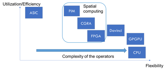
Figure 1:Neural Network Accelerator Architecture Paradigm
2.1 Comparison of FPGA and ASIC for Neural Network Implementation
Compared to ASIC, FPGA with the same logic functional characteristics at the same process node is slower, consumes more power, and has a higher unit cost: However, this is a necessary price to pay for the configurability of FPGA.
In contrast, designing and manufacturing ASIC takes a long time and is expensive, while FPGA can be obtained directly. Therefore, in small to medium-sized and high-value applications, FPGA is preferable to ASIC, as it can meet the required capacity and I/O functions, especially in cases where hardware needs to be flexible and reconfigurable.
An example of such applications is SmartNIC, for which both Xilinx and Intel provide dedicated products in AI scenarios.
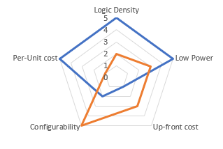
Figure 2: Comparison of FPGA and ASIC for NN Implementation
Since ASIC hardware cannot be reconfigured like FPGA, it is preferable to use flexible NPUs that can execute different models on ASIC, rather than hard-coded NPUs that only support optimization for specific models.
In ASIC, digital hardware modules that accelerate specific NN operators can be used alongside general-purpose NPU. Although the architecture of these modules is fixed, they can still be configured to some extent: for example, accepting different weights or executing one of a set of supported operators at any given time.
2.2 Comparison of FPGA and GPU/NPU for NN Implementation
GPUs and NPUs typically have a set of general-purpose processing units (tensor cores), and NN is deployed and executed by mapping it onto these processing elements (PEs) using dedicated compilers.
For models specifically optimized for FPGA, it may be more energy-efficient than GPU. This is because dedicated logic blocks can be designed for FPGA to reduce the computation required for specific models using fine-grained quantization while maintaining accuracy, whereas GPU/NPU only supports limited means of quantization.
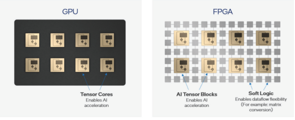
Figure 3: Some FPGA include tensor cores like GPU, and they also have programmable “soft” logic [2]
Modern GPU cards have a lot of very fast memory (e.g., equipped with GDDR), while FPGA has relatively less on-chip memory (e.g., “BlockRAM” in Xilinx devices). In order to store model weights, FPGA implementations typically use external DDR SDRAM. Generally speaking, the external memory used in FPGA implementations has a slower access rate than the memory used in GPU.
Even Intel and Xilinx admit that FPGA does not outperform GPU across all performance metrics. However, Intel also points out that compared to GPU, FPGA has advantages in low latency, hardware customization, interface flexibility, and power consumption. Objective evaluations conducted by Berten DSP have also reached similar conclusions, as shown in the figure below.
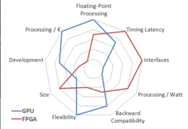
Figure 4: Performance Comparison Between GPU and FPGA – BERTEN (bertendsp.com)
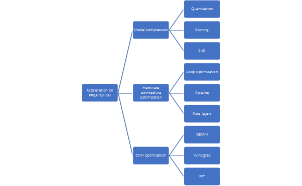
3. NN Model Optimization Techniques for FPGA
The literature [3] analyzes optimization techniques that can be used to prepare neural networks for implementation on FPGA (or ASIC):
1. Weight Quantization
2. Weight Pruning
3. Matrix Decomposition SVD
In cases where matrix multiplication is used, the number of weights and multiplications can be reduced by lowering the rank of the matrix using Singular Value Decomposition (SVD).
1. Loop Optimization
2. Data Flow
3. Layer Fusion
-
Reducing the complexity of convolution implementations, such as using FFT and Winograd methods
Figure 5:Neural Network Optimization Techniques Based on FPGA
3.1 FPGA for CNN Network Acceleration
As shown in Table 1, several typical CNN-based neural networks are listed along with their parameter scales and computational loads.
|
VGG16
|
MobileNet V1
|
ResNet-50
|
|
Comp.(GOP)
|
31.1
|
1.14
|
7.8
|
|
Param.(M)
|
138
|
4.21
|
25.5
|
Table 1: Several Typical CNN-based Neural Networks
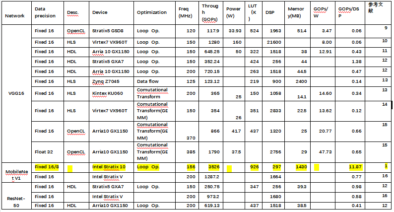
For the typical neural networks listed in Table 1, various FPGA implementation solutions for CNN networks have been collected.
Table 2: Comparison of FPGA Implementation Solutions for Several Typical CNN-based Neural Networks
From the above table, we can see that the literature 【1】 achieves the highest computational efficiency among all known papers targeting CNN, improving throughput and latency by 2-4 times compared to other closest FPGA implementation solutions, and achieving an inference speed of 3000FPS on the ImageNet dataset. The main reason is that the flattened data flow on FPGA combined with multi-precision mixed quantization and other hardware-software co-design greatly reduces the model size and computational complexity.
Currently, most CNN accelerators, including NPU, adopt a homogeneous large-scale pulsed array architecture. Using this architecture, multiple batches of images can be processed in parallel on different PEs or sets of PEs. NN layers can be processed sequentially by reusing the same hardware, with each layer having different configurations/weights. For example, NVIDIA GPUs include “tensor cores.” Moreover, both Xilinx and Intel offer FPGAs with dedicated AI modules for implementing PE arrays. The complexity of each PE can be adjusted: low-complexity PEs can consist of just a set of multipliers/accumulators, while higher complexity PEs can be small instruction-set programmable processors. As many different convolution layers reuse the same hardware computing units, the pulsed PE array is time-multiplexed. However, the varying input data sizes, channel counts, convolution kernel sizes, and the emergence of new convolution structures such as depthwise make it increasingly challenging to achieve efficiency on a single large computing core.
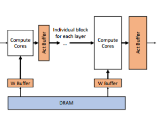
Therefore, the literature 【1】 adopts another hardware architecture approach, disassembling the CNN network by layers and streaming it to different computing units. Each computing unit is driven by input activation values, aiming to
|
PE (Tensor) Array NPU Architecture (for AI/Neural Processing Synopsys ARC NPX6 NPU Series)
|
Flattened NPU Architecture [1]
|
|
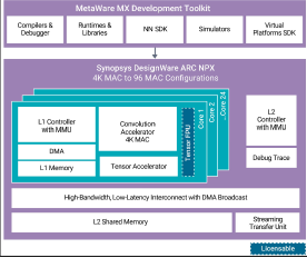
|
|
Figure 6:Large Pulsed PE Array and Flattened Architecture
As shown in the figure, the three different convolution layers (L1, L2, L3) are implemented differently on the homogeneous pulsed array and the flattened architecture. In the homogeneous pulsed array architecture, a large computing unit is used for convolution, while the flattened architecture uses three smaller computing units, C1, C2, and C3. Due to the differing sizes of the three convolution layers, using a single large homogeneous array architecture can lead to idle portions in the computing units, resulting in low hardware utilization. In contrast, the flattened architecture has multiple computing units of varying sizes to accommodate the dimensions of each convolution layer, thus fully utilizing hardware resources. As shown in the figure, the homogeneous array architecture requires four cycles to complete the computations of the three convolution layers, while the flattened architecture only requires two cycles.
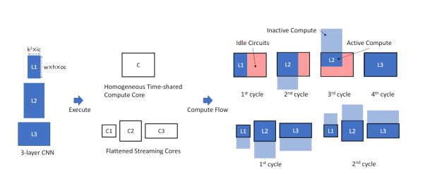
Figure 7:Implementation Differences of Homogeneous Pulsed PE Array and Flattened Architecture for Three Layers of Convolution
Based on the flattened architecture design, combined with mixed multi-precision quantization and more logic units in FPGA, or even cascading multiple FPGAs, the authors propose an automated tool framework that can map a complete CNN network onto FPGA. This framework first uses self-developed algorithms to perform fixed-point and offset search on pre-trained CNN models under various precisions, resulting in optimized models that meet accuracy requirements after quantization. Because the flattened architecture consists of multiple computing units, each unit can use different bandwidth precisions for quantization, ensuring minimal accuracy loss while compressing the model’s computational load. During this phase, the framework also accurately estimates hardware resources, including latency, LUT, and BRAM utilization rates, etc. Based on the generated optimized model and resource estimates, the framework generates systemVerilog using a pre-prepared verilog library, ultimately generating the FPGA hardware files after synthesis.
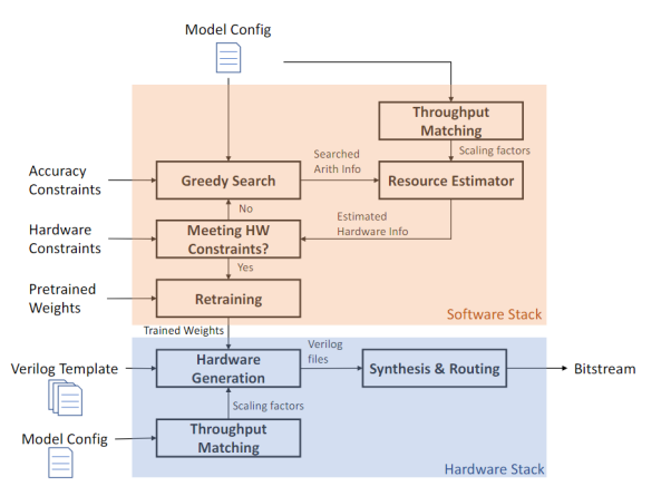
Figure 8:Automatically Generated Accelerator Framework Based on FPGA for a Neural Network
3.2 FPGA for Transformer Network Acceleration
As shown in Table 3, several typical transformer-based neural networks are listed along with their parameter scales and computational loads.
|
BERT base 128
|
ViT Base
|
Swin-T tiny
|
|
Comp.(GOP)
|
29
|
33.03
|
4.36
|
|
Param.(M)
|
110
|
86
|
28.29
|
Table 3: Several Typical Transformer-based Neural Networks
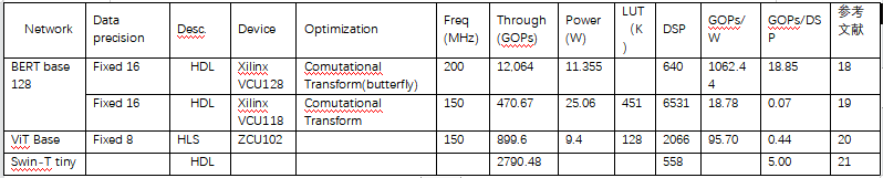
For the typical neural networks listed in Table 3, various FPGA implementation solutions for transformer networks have been collected.
Table 4: FPGA Implementation Solutions for Several Typical Transformer-based Neural Networks
Among the implementation solutions in the above table, the literature 【18】 achieves the highest power consumption and hardware efficiency, primarily optimizing the attention module and forward propagation network (FN, also known as Multi-Layer Perceptron (MLP)).
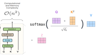
In the transformer network, the typical self-attention formula is expressed as shown in the figure below. In the self-attention module, for matrix multiplication, if the sequence length is n, the time complexity will be O(n^2), and it will also consume N^2 time and storage.
Figure 9: Typical Self-Attention Module Formula Expression and Schematic
The structure diagram of the forward propagation network (FN) is shown below, divided into input layer, hidden layer, and output layer. Each layer has several neurons, thus each layer will define weight matrices. The specific calculation details are not expanded here; the key point is that the computation between each layer is essentially also matrix-vector multiplication.
Figure 10: Typical Self-Attention Module Formula Expression and Schematic
In both the attention and FN modules, there are calculations for matrix-matrix multiplication and matrix-vector multiplication, and performing sparse decomposition on the matrix is an effective way to reduce the computational complexity and storage space of the matrix. That is, each matrix has a specific structure that can be represented in a compressed form, thus enabling a multiplication algorithm with lower complexity instead of consuming O(n^2) computational complexity for large matrix vector multiplication algorithms.
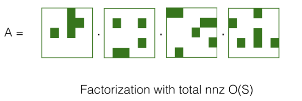
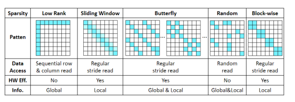
Figure 11:Sparse Decomposition of Matrices
As shown in the figure, there are currently various sparse schemes in academia to approximate matrix multiplication, including low-rank, sliding window, butterfly, random, and block-wise.
Figure 12:Several Mainstream Matrix Compression and Sparsity Methods
Choosing which matrix compression method to adopt mainly considers several factors. First, can the method capture both local and global information simultaneously in a single sparse mode? Second, can the sparse or compressed model be sufficiently hardware-friendly for design? Finally, can the sparse or compressed mode support both the needs of the attention mechanism and the forward propagation network FN?
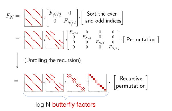
Comparing several matrix compression and sparsity methods, the butterfly matrix decomposition model can meet the above requirements, as the matrix can be represented by the product of log(N) sparse butterfly factor matrices, reducing the computational and memory complexity from O(N^2) to O(N log N).
Figure 13:Butterfly Matrix Sparse Decomposition Process
The literature 【17】 proposes a network architecture called FABNet, which is composed of two blocks, ABfly and FBfly. The ABfly module primarily implements the butterfly transformation, retaining the backbone of the attention module and compressing all linear layers using butterfly decomposition. The ABfly block starts with three butterfly linear layers to generate the Q, K, and V matrices, which are then input into a vanilla multi-head attention layer and another butterfly linear layer to capture relationships between different tokens, followed by additional processing by a butterfly forward propagation network (FN) composed of two butterfly linear layers. To further enhance hardware efficiency, in addition to ABfly, there is also the FBfly module in the network, which first performs a 2D Fourier transformation via Fast Fourier Transform (FFT) to effectively smooth different input tokens, allowing the subsequent butterfly forward propagation network (FN) to handle longer sequences. Although the Fourier transformation may lead to accuracy loss, it consumes less computation and storage compared to butterfly transformation. The quantities of the ABfly and FBfly modules in the network can be configured as hyperparameters to seek the best balance between accuracy and efficiency.
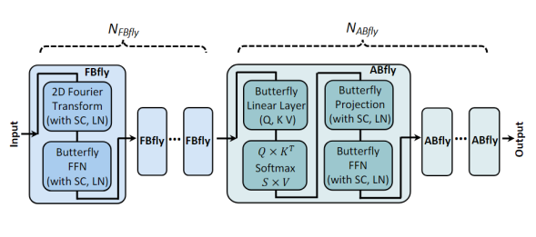 Figure 14:Illustration of FABNet Network Structure
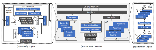
For the adaptive butterfly hardware accelerator architecture based on the transformer, as shown in the figure, it mainly consists of a Butterfly Processor (BP), Attention Processor (AP), Post-Processing Processor (PostP), and on-chip buffer, etc. The BP includes multiple Butterfly Engines (BE), primarily used to accelerate butterfly transformations and Fast Fourier transformations. The AP contains multiple Attention Engines (AE), each consisting of a QK unit and an SV unit. The QK unit is used to compute the matrix multiplication between queries and keys, as well as softmax, while the SV unit accepts outputs from the QK unit and multiplies them with the Value vector to produce the final result of the attention mechanism.
Figure 14:Illustration of FABNet Network Structure
For the adaptive butterfly hardware accelerator architecture based on the transformer, as shown in the figure, it mainly consists of a Butterfly Processor (BP), Attention Processor (AP), Post-Processing Processor (PostP), and on-chip buffer, etc. The BP includes multiple Butterfly Engines (BE), primarily used to accelerate butterfly transformations and Fast Fourier transformations. The AP contains multiple Attention Engines (AE), each consisting of a QK unit and an SV unit. The QK unit is used to compute the matrix multiplication between queries and keys, as well as softmax, while the SV unit accepts outputs from the QK unit and multiplies them with the Value vector to produce the final result of the attention mechanism.
Figure 15:Adaptive Butterfly Hardware Accelerator Architecture Based on Transformer
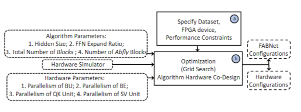
As mentioned earlier, the quantities of the ABfly and FBfly modules in the FABNet network can be configured as hyperparameters. Based on these two parameters, a hardware-software co-design method is developed, as shown in the figure, to achieve design space exploration for neural architecture and hardware design.
Figure 16:Hardware-Software Co-Design Framework Based on Adaptive Butterfly Hardware Accelerator Architecture
4. Conclusion
This article analyzes the comparison between FPGA, GPU, and ASIC. FPGA does not “beat” GPU and ASIC in all metrics for implementing NN. By listing various FPGA implementation solutions for neural network accelerators, as well as analyzing two specific instances targeting CNN and transformer based networks, it is shown that FPGA has unique advantages in the co-design of hardware and software, particularly in model quantization and sparsity. Even if the final product is commercialized in the form of ASIC, FPGA remains the best platform for ASIC digital logic prototyping, testing, and technical demonstration.
Welcome to all angel round and A-round enterprises in the entire automotive industry chain (including the electrification industry chain) to join the group(Friendly connections with 700 automotive investment institutions including top-tier institutions; Some quality projects will be selected for themed roadshows to existing institutions); There are communication groups for leaders of science and technology innovation companies , automotive industry complete vehicles, automotive semiconductors, key parts, new energy vehicles, smart connected vehicles, aftermarket, automotive investment, autonomous driving, vehicle networking, and dozens of other groups. Please scan the administrator’s WeChat to join the group (Please indicate your company name)