The key points and best practices for PCB layout design of Arduino open source hardware expansion boards.In the Arduino ecosystem, the PCB design of expansion boards (Shields) requires meticulous planning. This article will delve into the key technical points of PCB layout design for Arduino expansion boards, providing professional guidance for design engineers.1. Stacking Structure and Stacking DesignStandard Arduino expansion boards typically use a dual-layer PCB design, separating the signal layer from the power layer. For expansion boards with high-speed signals or complex functions, a four-layer structure is recommended:Top Layer: Signal layer and component layoutInner Layer 1: Power planeInner Layer 2: Ground planeBottom Layer: Signal layerStacking Distance ControlThe minimum distance between expansion boards should be maintained at over 10mm.Consider thermal requirements, leaving sufficient space around high-heat components.Connector heights should be controlled within standard ranges.2. Key Signal Routing StrategiesHigh-Speed Signal ProcessingSPI bus routing should be designed to be equal length, and differential pair routing should use serpentine compensation.Pull-up resistors for I2C signal lines should be placed close to the devices.Analog and digital signals should be routed in separate zones to avoid crosstalk.Power Integrity DesignUse a star topology for power distribution.Decoupling capacitors should be placed close to the power pins.Main power traces should have a width of over 3mm.Key components should have dedicated power filtering networks.3. EMC Design ConsiderationsGround Plane DesignA complete ground plane segmentation design.Analog ground and digital ground should be connected at a single point.Avoid ground plane slots beneath key signals.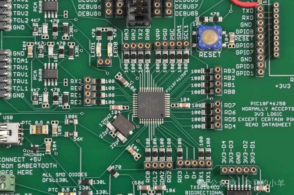 Shielding DesignGround vias should be arranged around high-frequency signal lines.Increase ground shielding in sensitive circuit areas.Leave space for shielding cover installation around key EMI components.4. Mechanical Structure OptimizationStandardized Interface LayoutStrictly follow the pin definitions for Arduino expansion interfaces.Leave sufficient mechanical mounting holes.Edge rounding treatment to ensure operational safety.Thermal DesignPower components should be placed at the edges of the PCB.Increase copper foil for heat dissipation under key heat sources.Leave space for heat sink installation if necessary.5. Manufacturing and Testing DesignDFM OptimizationTrace and pad spacing should meet process requirements.Via designs should meet plating process requirements.Leave automatic placement margins between components.Test Point LayoutLeave test points for key signals.Add test pads for power nodes.Leave space for programming download interface.Finally, the PCB design of Arduino expansion boards should also pay attention to the following details:Silkscreen layer markings should be clear, including device polarity and reference numbers.Mask layer openings should be reasonable to avoid cold solder joints.Leave an area of over 5mm at the edges without components.Copper area ratio should be controlled between 20%-80%.Through reasonable PCB layout design, not only can the reliability and compatibility of the expansion board be ensured, but also the overall performance and manufacturing yield of the product can be improved. In actual design, it is necessary to comprehensively consider multiple dimensions such as electrical performance, thermal performance, and EMC characteristics to achieve scientific layout and reasonable routing.21:07