In complex PCB design, there is a seemingly inconspicuous yet crucial “small role”—the jumper. It acts like a “bridge” in the circuit, silently connecting various components and solving layout challenges. But did you know? Improper use of jumpers can lead to the collapse of the entire circuit! Today, we will unveil the classifications, functions of jumpers, and key details that even seasoned engineers might overlook!1. What is a Jumper?
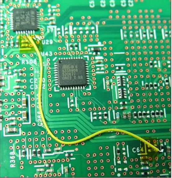
A jumper is a “circuit shortcut” achieved through thickened wires or special connections in PCB design, specifically addressing the following issues:
-
Components cannot be directly connected;
-
Components are too far apart;
-
Pin numbering errors need correction.
2. Four Major Classifications of Jumpers: How Many Have You Used?
-
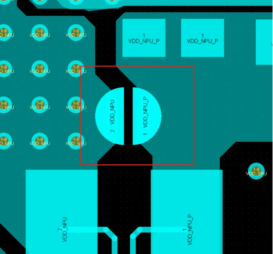
Copper Wire Jumper: Simple and direct, but layout interference must be considered;
-
Resistor Jumper: Stabilizes signals; the choice of resistance value is key;
-
Solder Jumper: Flexible but tests soldering skills;
-
PCB Jumper: Achieved through connection holes, offering high flexibility.
3. Three Core Functions of Jumpers
-
Connecting Complex Circuits: Like a “circuit matchmaker”, solving the “long-distance relationship” of components;
-
Signal Separation: Avoiding interference in high-power circuits;
-
Improving Reliability: Reducing failure rates and making designs more stable.
4. “Death Traps” in Jumper Usage
While jumpers are beneficial, falling into these traps can ruin the entire design!
-
Jumpers that are too long or coiled → Signal attenuation;
-
Improper positioning → Interference with other circuits;
-
Weak soldering → Intermittent circuit connection;
-
Incorrect grounding → Causes noise.
5. Essential Rules for Jumper Design for Engineers
-
Short and Straight: Keep lengths as short as possible to avoid winding;
-
Away from Sensitive Signals: Such as high-frequency or analog circuits;
-
Check Soldering: Use a magnifying glass to confirm solder joint quality;
-
Test and Validate: Use a multimeter to check connectivity before powering on.
Conclusion:Though small, jumpers are the “invisible MVP” in PCB design. Mastering their correct usage can make your circuit design much more efficient! What pitfalls have you encountered with jumpers? Feel free to share in the comments!

[Recommended Material] Essential Secrets for Switching Power Supply Design! Complete Guide to PCB and Layout Optimization
2025-08-21
What is the purpose of the 1MΩ resistor in the crystal oscillator circuit? How to choose it?
2025-08-21
How to adjust the topology of a PCB to improve signal integrity?
2025-08-21

Scan to add customer service WeChat, note “Join Group” to pull you into the official Fanyi Education technical WeChat group, where you can exchange technical issues and insights with many electronic technology experts~
Share, Like, and Support with a “Three-Click” ❤️