
This article is reprinted from the WeChat public account: FPGA Algorithm Engineer
We all know that recently, the topics of chip design and manufacturing continue to occupy people’s conversations. The enemy’s pursuit has made us abandon our fantasies and fight back. In our work and life, whether we are in the upstream or downstream of the semiconductor industry, we cannot avoid chips; without them, we cannot move an inch.
When you are at home with the air conditioning on, taking a bottle of ice-cold cola from the refrigerator, and lounging on the sofa scrolling through videos on your phone, you hope the video streams smoothly without lag. Behind this, there is a group of chip design engineers, mobile communication engineers, network engineers, image processing engineers, chip development/verification engineers, chip manufacturing engineers, and chip packaging and testing engineers… working tirelessly day and night.
Any chip design requires a large design and verification team to closely collaborate to complete it. In chip design, we need to consider many factors. So, what are we thinking about?
The three realms of chip logic development engineers: a circuit in mind, timing in brain, and code in hand.
If we use synchronous design or any IP in our design, or finalize the architecture and microarchitecture, we need to establish various strategies. Below are some of them:
-
Functionality and compatibility of the design
-
Parallelism, concurrency, and pipelining strategies
-
External IO and high-speed interfaces
-
Area and initial gate count estimation of the design
-
Speed and maximum frequency requirements
-
Power consumption requirements and use of low-power designs
-
Clock network and delay
-
Interface and IO delay and modeling strategies
After considering the above, a team of experienced technicians will finalize the architecture and microarchitecture of the ASIC/SOC design.
To facilitate understanding of the architecture and project development, we need to consider some design factors, mainly in the following aspects.
01
Timing Parameters
The important timing parameters of the rising edge-sensitive flip-flops are shown in Figure 1, which are:
-
Setup time (tsu)
-
Hold time (th)
-
Trigger propagation delay (tpd)
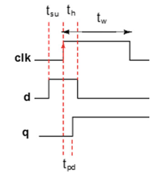
Figure 1 Timing parameters of D flip-flop
Setup time (tsu): The minimum time that the data input of the flip-flop should remain stable before the active edge of the clock arrives is called setup time.
The active edge refers to the rising edge (positive edge) sensitiveD flip-flop transitioning from low to high, and the falling edge (negative edge) sensitiveD flip-flop transitioning from high to low.
If the data input changes from 1 to 0 or vice versa during the setup time window, the flip-flop output will be metastable, indicating a setup violation.
Hold time (th): The minimum time that the data input of the flip-flop should remain stable after the active edge of the clock arrives is called hold time.
The active edge refers to the rising edge (positive edge) sensitive D flip-flop transitioning from low to high, and the falling edge (negative edge) sensitiveD flip-flop transitioning from high to low.
If the data input changes from 1 to 0 or vice versa during the hold time window, the flip-flop output will be metastable, indicating a hold violation.
The propagation delay of the flip-flop (tpd=tcq): The time required for the flip-flop to produce a valid output after the active edge of the clock is called the propagation delay of the flip-flop.
Propagation delay is also referred to as the clock to Q delay, also known astcq.
02
Metastability
If the data input of the design shown in Figure 2 is connected to another module whose clock is generated by a different clock source, the output of the first flip-flop will be in a metastable state.
Meta_data indicates that the flip-flop data is in a metastable state, thus the first flip-flop experiences a timing violation. Metastability indicates that the data output is invalid, and to obtain valid data output, the design needs to use multi-level synchronizers.
The timing of the data sampled by the first flip-flop and the output of the second flip-flop is shown in Figure 3. As illustrated, the output of the first flip-flop is in a metastable state, while the output of the flip-flop’sdata_out is in a valid state.
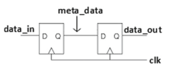
Figure 2 Level Synchronization
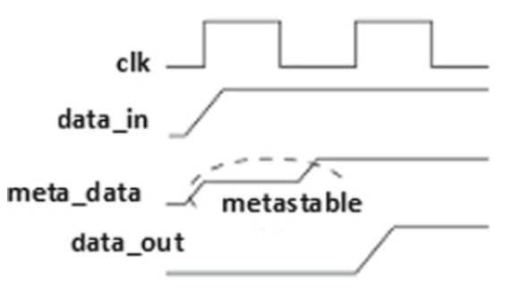
Figure 3 Timing of Metastable Level Synchronization
03
Clock Skew
If there are multiple clocks in the ASIC design, then clock distribution and clock tree synthesis will play a very important role in balancing the clock skew between different clock inputs of various blocks.
If two different clocks in the design arrive at different time instances, then the design has clock skew. The cause of clock skew is routing delay, which is the line delay of a single clock domain design. Considering the illustrated diagram, let us consider the clock of the transmitting flip-flop arriving at time instancet0, and the capturing flip-flop at time instancet2. Due to the different arrival times of the clock in this synchronous design, there is a phase shift betweenclk1 andclk2, which we can regard as clock skew. Another reason is the aging of the oscillator; hence, the frequency of the clock cycle produced by the oscillator changes, and the difference in arrival times can be referred to as jitter.
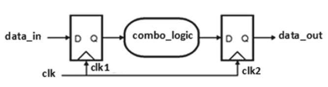
Figure 4 Synchronous Design
In Figure 4, the clock skew is caused by the interconnect delay betweenclk1 andclk2 pins.
In practical ASIC design, we experience two different types of skew as shown in Figure 5.
Positive Clock Skew: Indicates that the transmitting clockclk1 is triggered first, and then the capturing clockclk2 arrives. As shown in the figure,tskew is the difference in arrival times betweenclk1 andclk2. In other words, we can imagine that positive clock skew is when data and clock run in the same direction, positive clock skew is beneficial for setup time but detrimental for hold time, as there is a positivemargin to manage.
Negative Clock Skew: Indicates that the transmitting clockclk1 is triggered last, while the capturing clockclk2 is triggered first. As shown in the figure,tskew is the difference in arrival times betweenclk1 andclk2. In other words, we can imagine that negative clock skew is when data and clock run in opposite directions, negative clock skew is better for hold time but detrimental for setup time.
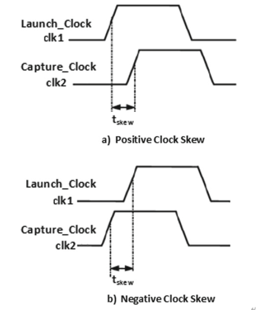
Figure 5 Skew in Design
In ASIC design, we always encounter clock skew caused by jitter or interconnect (i.e., line delay), below are the key points we should know.
-
Positive clock skew is beneficial for setup time but detrimental for hold time.
-
Negative clock skew is beneficial for hold time but detrimental for setup time.
Positive Clock Skew
As discussed earlier, positive clock skew indicates that the transmitting flip-flop is triggered first, then the capturing flip-flop is triggered. There is a buffer delay margin between the transmitting clock and the capturing clock that can be used to improve the frequency required by the design.
Figure 6 shows the synchronous design with positive clock skew, the skew betweenclk1 andclk2 istbuffer.
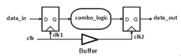
Figure 6 Positive Clock Skew
Let’s identify the required data time and data arrival time.
Data Arrival Time (AT)=tpff1+tcombo
Data Required Time (RT)=Tclk+tbuffer-tsu
Where,Tclk is the clock cycle or clock to Q delay.tbuffer is the buffer delay,tsu is the setup time of the flip-flop,tpff1 is the propagation delay of the flip-flop,tcombo is the combinational logic delay.
Setup slack is the difference between the data required time and data arrival time, which should be positive. A positive setup slack indicates that there are no setup violations in the design. To avoid setup violations in the design, it should have fast data, a fast launching clock (clk1), and a slow capturing clock (clk2). In other words, the actual arrival of data should be faster than the required data time. (As shown in Figure 7)
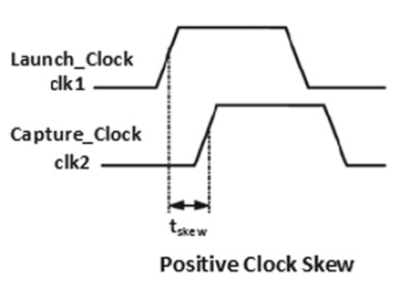
Figure 7 The relationship between launch and capture clocks for positive clock skew
Negative Clock Skew
As discussed earlier, negative clock skew indicates that the transmitting flip-flop is triggered last, while the capturing flip-flop is triggered first. The buffer delay margin between the launching clock and capturing clock reduces the maximum frequency of the design.
Figure 8 shows the synchronous design with negative clock skew, the skew betweenclk1 andclk2 istbuffer.
Let’s identify the required data time and data arrival time.
Data Arrival Time (AT)=tbuffer+tpff1+tcombo
Data Required Time (RT)=Tclk-tsu
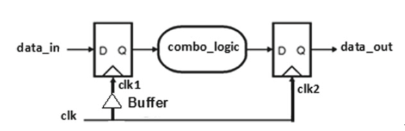
Figure 8 Negative Clock Skew
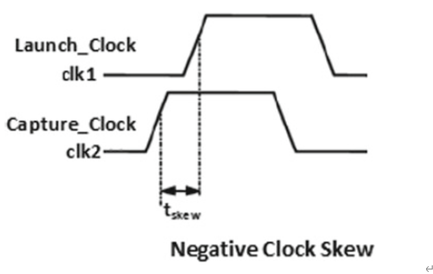
Figure 9 The relationship between launch and capture clocks for negative clock skew
04
Slack
In ASIC design, there are two terms used to describe slack, namely setup slack and hold slack.
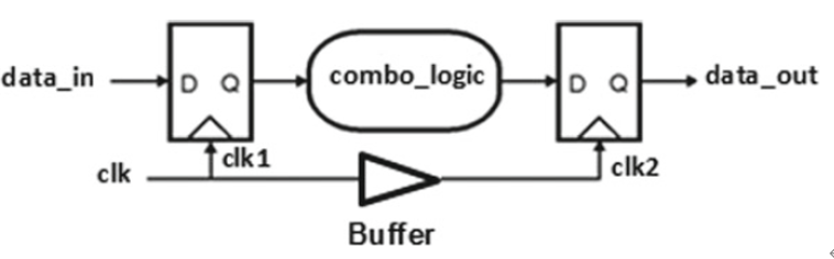
Figure 10 Register to register path in synchronous design
Setup Slack
Setup slack is the difference between the data required time and data arrival time, which should be positive. A positive setup slack indicates that there are no setup violations in the design.
Data Arrival Time (AT)=tbuffer+tpff1+tcombo
Data Required Time (RT)=Tclk-tsu
Setup Slack=RT-AT
Hold Slack
Hold slack is the difference between data arrival time and data required time, which should be positive. A positive hold slack indicates that there are no hold violations in the design.
05 Clock Delay
The clock is generated by a phase-locked loop for single clock domain designs, and for multiple clock domains, we may need multiple phase-locked loops.
The clock network introduces delay, which is actually the time required for the clock to reach the chip, and the clock delay is caused by the clock network delay during the clock distribution process.
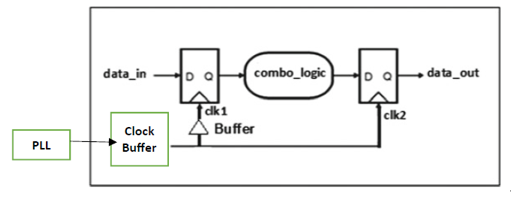
Figure 11 Clock network delay
06
Area of Design
The total area of an ASIC consists of standard cells, macros, andIP cores. In designs with millions or billions of gates in integrated circuits, area constraints and better layout planning play a significant role in achieving the expected performance. We can consider area optimization at different design stages, such as:
-
During the architecture design process, obtaining better strategies through interaction descriptions of different functional blocks.
-
During the RTL design process, using tool-based instructions and commands, and employing resource-sharing techniques.
-
In the physical design stage of layout, placing functional blocks using strategies to minimize area consumption caused by routing delays and routing resource usage.
07
Speed Requirements
In ASIC design, speed is another important consideration. Various speed improvement techniques can enhance the performance of the ASIC. For instance, considering that the processor design works at a frequency of500MHz, we face the challenge of increasing the design frequency. In this case, various strategies can be employed during the ASIC design cycle, but may be used sparingly:
-
During architecture and microarchitecture design, having better sequential boundary definitions.
-
In the initial layout, placing interdependent blocks closely together to minimize area, thus reducing routing delays and enhancing speed.
-
During the RTL design phase, using balanced registers and register replication, optimization commands to enhance design performance. However, these may impact logical area.
-
During the RTL design process, utilizing input and output of registers to improve design performance.
-
Using pipelining concepts and architectures whenever feasible.
-
If FSM design and controllers are needed in the design, work on control and data path synthesis for clean timing and better performance.
-
Prefer synchronous designs as they are faster than asynchronous designs.
-
Avoid internal clock generators as much as possible; instead, consider clock trees and optimize the clock tree during CTS.
-
During the routing phase, attempt to use tool-based enhancement techniques, as enabling tool instructions can play a particularly important role in balancing clock skew.
08
Power Requirements
For any type ofASIC orSOC design, an important consideration is power, and the design team’s goal is to reduce leakage and dynamic power. Power planning is conducted with power constraints during the physical design process. During different stages of the ASIC design flow, power optimization techniques should be employed.
-
ASIC architectures with low-power awareness.
-
Using UPF at different design levels.
-
During RTL, using dedicated clock gating units to minimize dynamic power.
-
Power optimization during RTL stage by avoiding unnecessary data value assignments and transitions.
-
Better power planning and power sorting for multiple power domains during the physical design process.
-
Better power-down strategies during the physical design process.
09
Design Constraints
Design constraints are essentially design rule constraints and optimization constraints. We can consider these constraints as module-level constraints, top-level constraints, and chip-level constraints.
Design Rule Constraints (DRC): We can view these constraints as the rules of the chip manufacturer that should be satisfied. During the physical design process, we will check if all theDRC check rules of the chip manufacturer are met. Layout is clean indicates noDRC violations. These constraints mainly include:
-
Transition
-
Fanout
-
Capacitance
Optimization Constraints: These constraints are used during the design and optimization phases. These constraints mainly include
-
Area
-
Speed
-
Power
Mainly using Synopsys DC, we will utilize area and speed constraints and attempt to optimize the design at various optimization stages.
Physical design tools, such as Synopsys IC Compiler, leverage area, speed, and power constraints to meet the final constraints for a clean chip layout.


E Course Network (www.eecourse.com) is a professional integrated circuit education platform under Moore Elite, dedicated to the cultivation of high-quality integrated circuit professionals in the semiconductor industry. The platform is oriented towards the job requirements of integrated circuit companies, providing a practical training platform that aligns with the corporate environment, quickly cultivating students to meet corporate needs.
E Course Network has a mature training platform, a complete curriculum system, and a strong faculty, planning a total of 168 high-quality semiconductor courses in China, covering the entire integrated circuit industry chain, and has 4 offline training bases. To date, it has deeply trained a total of 15,367 people, directly supplying 4,476 professional talents to the industry. It has established deep cooperative relationships with 143 universities and has held 240 corporate-specific IC training sessions.