
The recent incident where Huawei’s Kirin chips were blocked by the United States has barely passed, and now Xiaomi has encountered issues.
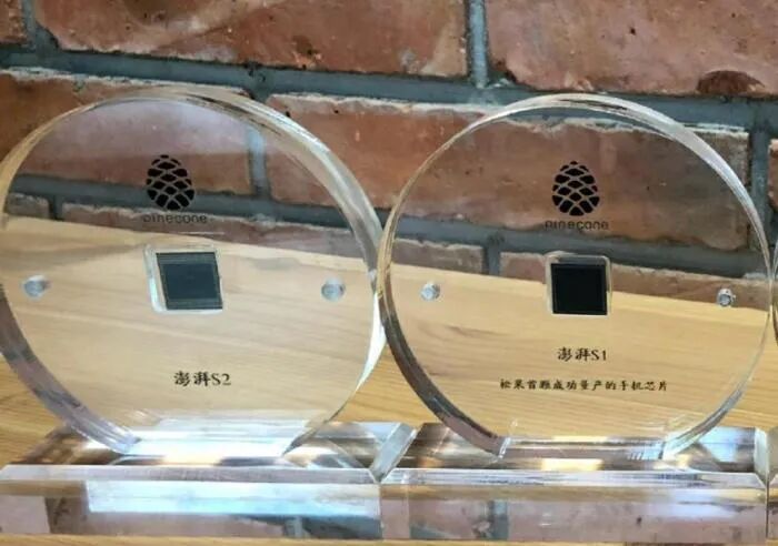
On August 9, Lei Jun suddenly posted on Weibo, responding to several questions that netizens were most concerned about, including the development progress of the Surge S2 chip. Lei Jun stated: The Surge S2 project is still ongoing, but it has encountered significant difficulties.
Although it was only a few short sentences, seeing Lei Jun’s response made me feel a mix of emotions. On one hand, the Surge S2 chip project, which had almost been forgotten by most people, is still persisting. On the other hand, the difficulties faced by the Surge S2 may be beyond our imagination, and it is likely to be very difficult to achieve mass production anytime soon.


Although Lei Jun did not mention the specific difficulties encountered, I speculate that it is likely related to chip manufacturing processes. In the previous article, I mentioned that domestic companies are currently unable to manufacture the photolithography machines necessary for producing high-end chips.
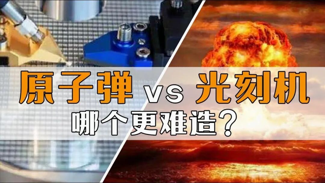
I even saw a viewpoint online: In the early days of the founding of the country, when we were poor and blank, we managed to develop two bombs and one satellite with our wisdom. Is it really harder to make chips and photolithography machines than to create an atomic bomb? It doesn’t make sense! If necessary, we should even draw by hand to produce high-end chips.

Emmmm, having such courage is certainly a good thing, but I must say that those who have this idea are too young and too simple.  Simply drawing by hand will definitely not produce chips, but this metaphor is quite appropriate. The photolithography machine is like the brush used for painting or the chisel used for carving; it is an indispensable tool in chip production!
Imagine, without a brush, how can you paint? No matter how high your skill level is, it would be futile. So, is making a photolithography machine really harder than creating an atomic bomb? Hold on, today I will explain to you how difficult it is to manufacture high-end photolithography machines and high-end chips.
First of all, high-end photolithography machines are known as the crown jewel of the modern semiconductor industry. A 7nm EUV photolithography machine consists of over 100,000 parts. These parts involve more than 200 industries! Including design, materials, optics, mechanics, algorithms, and integrated circuits, etc. So, does our country have these supporting industries? To be honest, yes, but not all, and compared to international advanced levels, the gap is still very large.
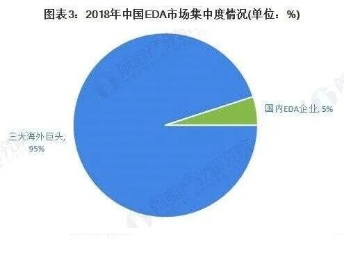
Taking the integrated circuit industry as an example, a picture illustrates the problem:
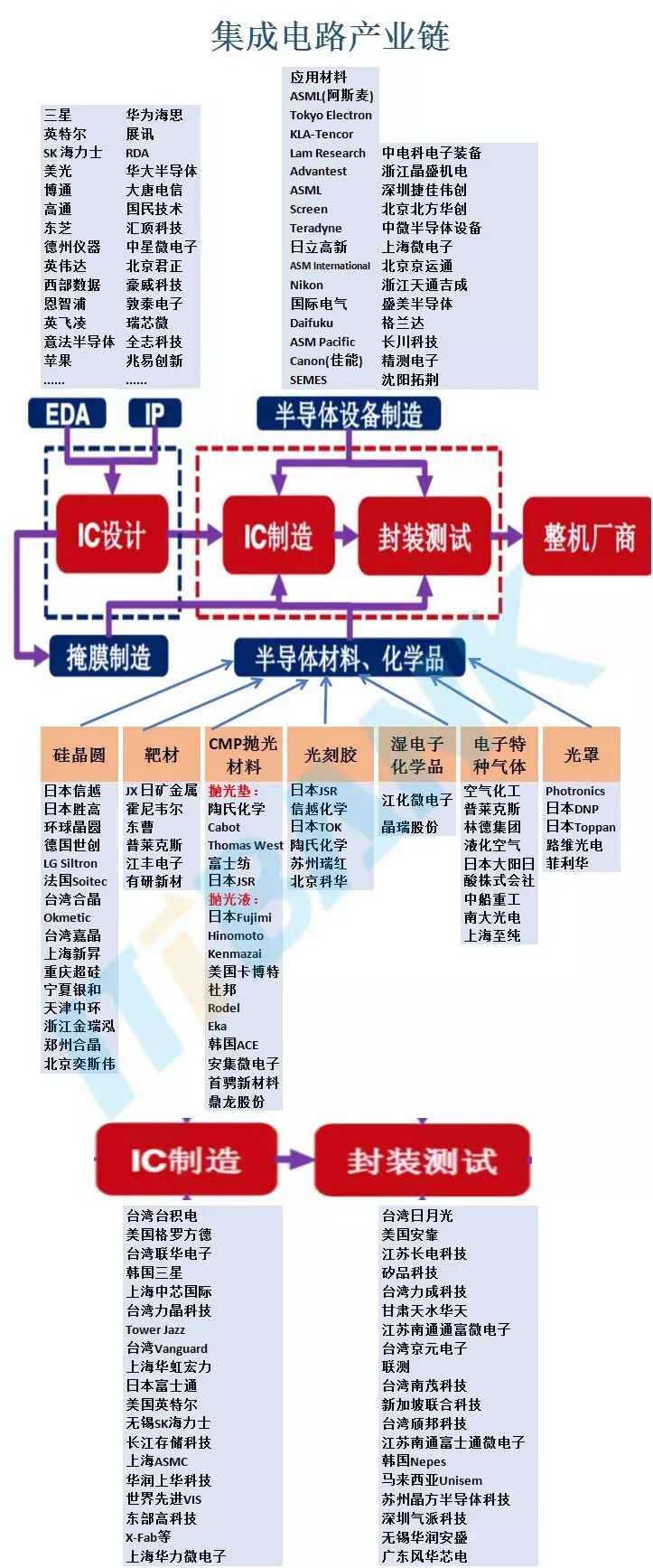
Have you noticed that in the semiconductor industry, European and American companies occupy a large portion, while Chinese companies are few and weak, with the real industry oligarchs almost all being European and American companies? Especially in semiconductor materials and IC manufacturing, our shortcomings are particularly obvious. There is really no harm in comparison…

Next, let’s look at a diagram of the semiconductor chip manufacturing process and industry chain:
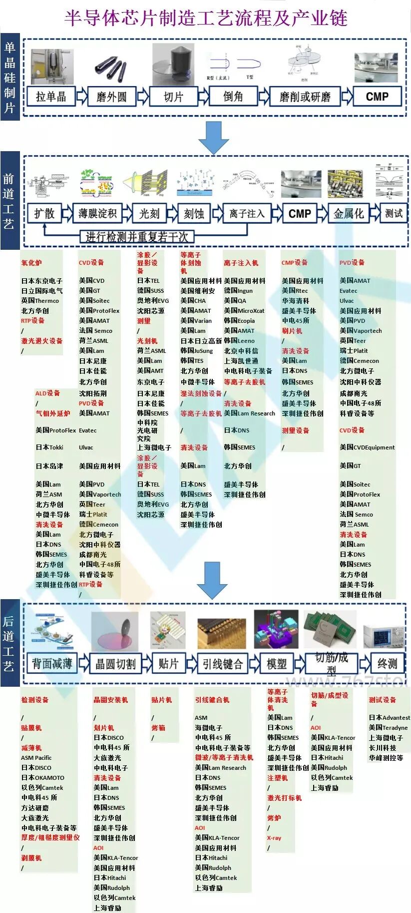
In every link, European and American companies dominate. I feel depressed…
If you think this is not enough to reflect the difficulty of manufacturing photolithography machines, then let me give a few specific examples:
The lenses used in ASML’s EUV photolithography machines are each the size of a frying pan, with almost insane requirements for the flatness and light transmittance of the lenses: more than 20 lens pieces stacked together must have extremely high light transmittance, and the surface of the lenses must be made to be nearly absolutely smooth.
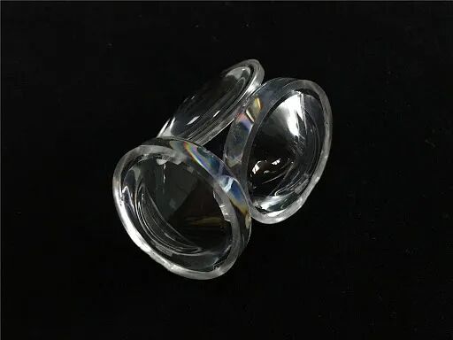
The lenses used in ASML’s EUV photolithography machines come from the top German optical giant Carl Zeiss. Currently, only Carl Zeiss in the world can produce such high-precision lenses for photolithography machines. Moreover, many of these lenses require manual polishing, and many engineers at Zeiss spend their entire lives doing this, with even their ancestors having done this for generations, accumulating over a hundred years of technology and experience.

And China clearly does not have an optical giant like Zeiss. Not to mention comparing with Zeiss, even compared to Japan’s Canon and Nikon, we are still far behind. Canon and Nikon can only produce low-end photolithography machines, let alone us. An ASML engineer once told a Chinese inspection team: even if we give you the complete set of blueprints, you still cannot produce it. 
This statement sounds very frustrating! But what they said is the truth; the gap in materials and processes cannot be solved by just a blueprint. What is needed is long-term accumulation and sedimentation, as well as the so-called craftsmanship spirit.
Furthermore, from DUV to EUV, the wavelength of ultraviolet light has sharply decreased from the original 193mm to 13.5mm. This requires 20KW of laser to strike a 20-micron tin droplet at a frequency of 50,000 times per second, vaporizing the liquid tin into plasma. This is equivalent to hitting a fly with a ping pong ball at a frequency of 50,000 times per second in a hurricane. The difficulty is unimaginable.

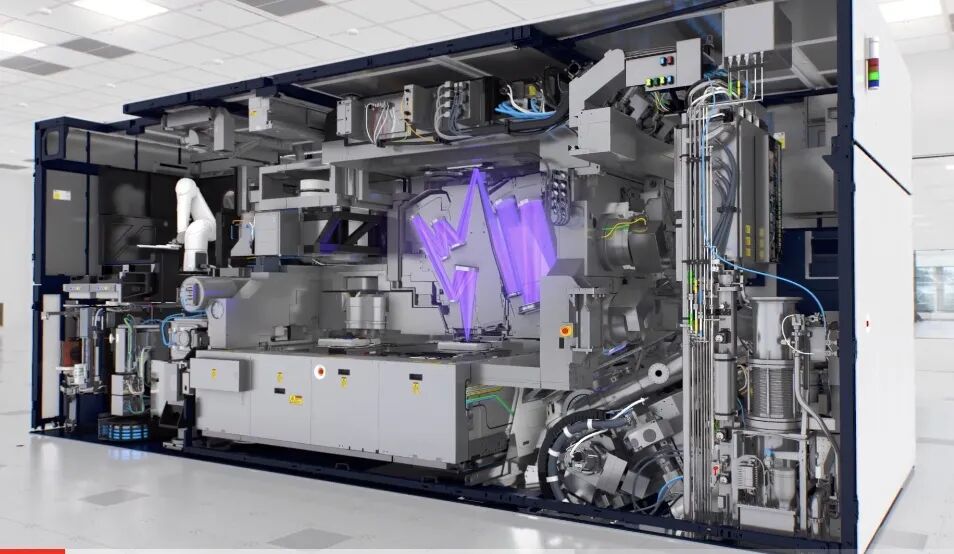
Therefore, it is not an exaggeration to say that the difficulty of manufacturing high-end photolithography machines is indeed comparable to that of an atomic bomb! Currently, our country is temporarily unable to produce high-end EUV photolithography machines due to backwardness in materials, technology, and other aspects.
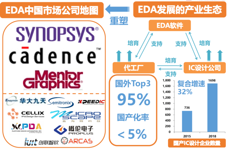
Having discussed photolithography machines, let’s talk about another major shortcoming of our country: EDA software. Many people do not understand what EDA software is. Simply put, EDA software is the software used to design chips, just like the PS software and necessary materials used by designers. Without software like PS or lacking essential materials, how do you think designers would manage?

EDA software is equivalent to the PS and materials for chip designers. Without EDA software, chip design is simply out of the question. A chip has tens of billions of transistors; it cannot all be drawn by hand. Currently, domestic EDA software is still relatively backward, with the three giants of American EDA software: Synopsys, Cadence, and Mentor Graphics occupying 95% of the domestic market share, which is not an exaggeration to call a monopoly.
EDA software has become the weakest link in China’s semiconductor industry. The core of EDA software lies in the underlying algorithms, and innovating at the algorithmic level is very difficult. It further involves theoretical innovations in foundational disciplines such as mathematics and physics. Currently, only Tsinghua University and Fudan University offer related majors in EDA software algorithms.

Those engaged in EDA software development need to be proficient in mathematics, physics, the semiconductor industry, mechanics, and other fields. Such composite talents are already scarce, and coupled with the fact that our country did not focus on cultivating talents in this area in previous years, it has led to a significant talent gap in the EDA field.
Therefore, there is a huge talent gap in the field of EDA software development in China, and due to various reasons, including “you know what,” European and American countries have implemented strict technological blockades against us in this field. This has resulted in China being significantly behind Europe and the United States in EDA software and related algorithms.

In contrast, the three giants of American EDA software: Synopsys, Cadence, and Mentor Graphics, started early, have a first-mover technological advantage, and have established extremely high technical barriers through decades of accumulation, making it very difficult for other companies to surpass them.
At this point, it is clear that China is very backward in both the hardware and software necessary for chip manufacturing, making high-end chip manufacturing a castle in the air, or even out of the question. So should China just give up?

Of course not! We not only cannot give up but must find a way to break the deadlock!
But how to break the deadlock? Given the current situation, our software and hardware are lacking, but it is not so pessimistic.
Careful readers may ask: Since making photolithography machines is as difficult as creating atomic bombs and involves over 200 supporting industries, if China cannot produce them, can the United States? Hey, good question! The answer is obvious: The United States cannot produce photolithography machines either! You see, ASML is a Dutch company, which indicates the problem. Moreover, the parts of their photolithography machines are sourced from dozens of different countries.

So even the current technological hegemon, the United States, cannot produce photolithography machines relying solely on its own strength. Not to mention, does the United States have an optical giant like Carl Zeiss? No, it does not! Therefore, at this stage, the United States also cannot produce photolithography machines.
So, if the United States cannot produce photolithography machines, is there a possibility for China to break the deadlock and ultimately overcome this challenge?
The answer is definitely yes! The reason is that China has the most complete industrial system in the world, which the current United States does not possess. In fact, there were once three countries in the world with complete industrial systems: China, the United States, and the former Soviet Union. However, after the Soviet Union collapsed, the United States focused on developing high-tech industries after World War II, abandoning many heavily polluting and inefficient heavy industries. Today, China has become the only country in the world with a complete industrial system.
Do not underestimate this complete industrial system; it is the foundation of a country’s high-end manufacturing industry! China’s ability to become a “construction madman” in recent years is due to our complete industrial system. And when it comes to infrastructure, the United States is just a little brother, only able to call us “dad.”

China, the construction madman
Don’t believe it? The gantry crane used to build the Ford-class aircraft carrier in the United States was manufactured by Shanghai Zhenhua Heavy Industry!
I have always believed that having a complete industrial system is a very powerful capability. It sounds simple to say, but it is very difficult to achieve. Without going far, just look at how China built the Leishenshan and Huoshenshan hospitals in just 10 days during this pandemic, and you will understand the power of a complete industrial system. This time we can also confidently say: even if we give you the complete set of blueprints, you still cannot produce it. 
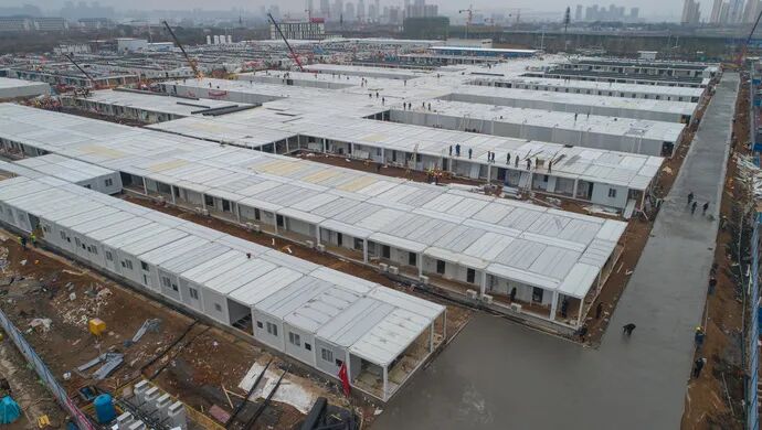
Leishenshan Hospital
Alright, I have gone a bit off track again. Let’s return to the research and manufacturing of photolithography machines. With a complete industrial system, we have the foundation to impact high-end manufacturing! We can develop various parts required for photolithography machines based on this foundation.
Relying on this complete industrial system, China can completely overcome various difficulties and ultimately produce high-end EUV photolithography machines. At that time, China is expected to become the only country in the world capable of independently manufacturing EUV photolithography machines solely with its own strength! This is certainly something to look forward to.
I am not saying this without basis; in fact, Shanghai Microelectronics has already achieved mass production of 90nm photolithography machines, and in 2021, it can deliver 28nm photolithography machines, with 22nm photolithography machines also under development. Do not underestimate these backward photolithography machines; at least they can prevent us from being choked in the mid-range chip market, so even though they are backward, we cannot do without them!
Let’s also take a look at domestic EDA software. Currently, the best EDA software in China is from Huada Jiutian. The first EDA software in China, the Panda system, was developed by Huada Jiutian. Although Huada Jiutian currently cannot compete with the three giants of American EDA software, with the rise of the domestic chip and semiconductor industries in recent years, EDA software has once again received national attention, which is undoubtedly a positive signal.

In fact, Chinese people are not that bad at software. Remember WPS? It was leading Microsoft Office at the end of the 1980s. In the DOS era, Qiu Bojun developed WPS by himself, dominating the word processing world.

Therefore, although China is still very backward in high-end chips and supporting software and hardware, we are not without solutions. On the contrary, China has asymmetric advantages in many areas. As long as we can make good use of these advantages, we can break the deadlock and ultimately become a strong chip nation. Who knows, with the development of China, Taiwan Semiconductor Manufacturing Company might one day become China Semiconductor Manufacturing Company. Hehe~
I, like all of you, look forward to the rise of China’s high-end chip industry! 