Dry Etching: Using gaseous chemical etchants to react with materials to form volatile by-products that can be removed from the substrate, achieving the purpose of etching.
Role of Plasma:
-
Generates free radicals, enhancing the rate of chemical reactions;
-
Simultaneously possesses ion bombardment capability, which can physically remove materials from the surface and break chemical bonds of surface atoms, significantly increasing the rate of chemical reactions during etching;
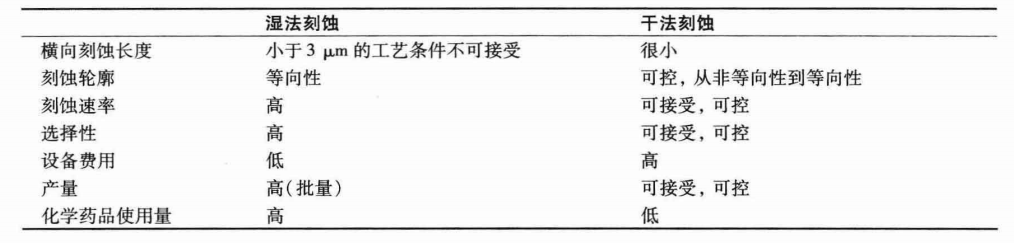
Comparison Table of Dry Etching and Wet Etching:
1. Classification of Etching
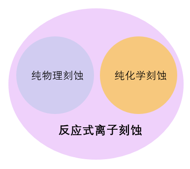
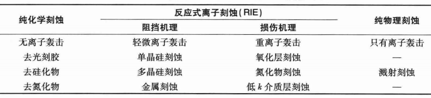
1. Pure Chemical Etching
No physical bombardment occurs, and material is removed through chemical reactions.
Includes wet etching and plasma photoresist removal processes.
Main Applications: Stripping processes, such as photoresist removal, silicon nitride removal, and removal of sacrificial layers.
2. Pure Physical Etching
Generally uses argon bombardment.
Pure physical etching rates are generally low, and selectivity is also low;
Main Applications: Dielectric sputter-back etching (to smooth openings for subsequent fill); cleaning before metal PVD, removing oxides to reduce contact resistance;
3. Reactive Ion Etching (RIE)
A more precise term should be ion-assisted etching, as ions may not necessarily undergo chemical reactions during this etching process. For example, in many cases, argon ions are used to enhance ion bombardment. As an inert atom, argon ions do not chemically react. The chemically active species in most etching processes are neutral free radicals. In semiconductor etching plasma, the concentration of neutral free radicals is much higher than that of ions. This is because the ionization activation energy is significantly higher than the dissociation activation energy, and the concentration of species is exponentially related to the activation energy. However, the term RIE has been used in the semiconductor industry for a long time, and it is unlikely anyone will change it.
The following diagram shows the principle of ion-assisted etching:
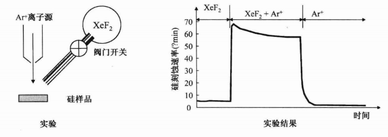
First, XeF2 gas is injected separately through a locking valve. XeF2 is an unstable gas. Xenon is an inert gas, so it does not form chemical bonds with other atoms. It is commonly used in dry chemical etching to deliver fluorine free radicals. When XeF2 contacts heated single-crystal silicon, it decomposes and releases two fluorine free radicals. Because fluorine free radicals have one unpaired electron, they can easily react chemically by gaining an electron from other atoms. Fluorine reacts with silicon on the sample surface to form volatile silicon tetrafluoride (SiF4). The measurement results in the diagram indicate that the etching rate of this pure chemical etching is quite low.
Next, the argon ion gun is turned on. Combining physical ion beam bombardment and chemical etching with fluorine free radicals significantly increases the etching rate of silicon. When the valve is closed to stop the flow of XeF2, silicon is solely etched by argon ion sputtering. This is a pure physical etching, and the etching rate is slower than that of the pure chemical etching using XeF2 flow.
As seen in the diagram, the etching rate when combining XeF2 flow and argon ion bombardment is the highest, significantly exceeding the sum of the etching rates when these two processes are used separately. The reason is that argon ion bombardment breaks the chemical bonds of surface silicon atoms, forming dangling bonds. Silicon atoms with dangling bonds are more likely to react with fluorine free radicals to form silicon tetrafluoride. Since ion bombardment is primarily in a vertical direction, the etching rate in the vertical direction is higher than that in the horizontal direction, so RIE exhibits anisotropic etching profiles.
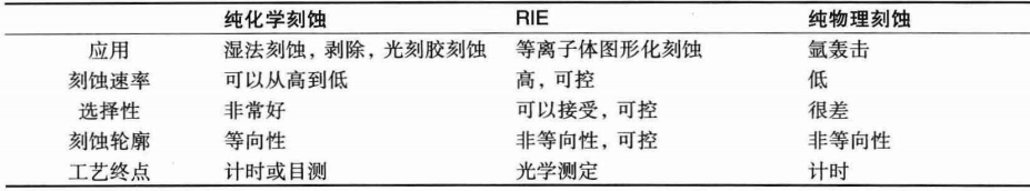
In advanced semiconductor manufacturing, almost all patterned etching is performed through the RIE process. The etching rate and selectivity of RIE can be controlled, and the etching profile is anisotropic and controllable. The following diagram compares these three etching processes:
2. Principles of Etching Processes
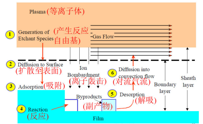
The plasma etching process is shown in the following diagram:
-
In plasma etching, the etching gas is first injected into the vacuum reaction chamber.
-
Once the pressure stabilizes, radio frequency is used to generate glow discharge plasma.
-
Some etchants decompose after being struck by high-speed electrons, generating free radicals, which then diffuse to the wafer surface beneath the boundary layer and are adsorbed onto the surface.
-
Under ion bombardment, free radicals quickly react with surface atoms or molecules to form gaseous by-products.
-
Volatile by-products that desorb from the wafer surface diffuse through the boundary layer into the convective flow and are expelled from the reaction chamber.
The principle of anisotropic plasma etching:
Due to ion bombardment in plasma etching, anisotropic etching profiles can be achieved, with two principles for anisotropy: damage mechanism and blocking mechanism, both related to ion bombardment.
-
Damage Mechanism:
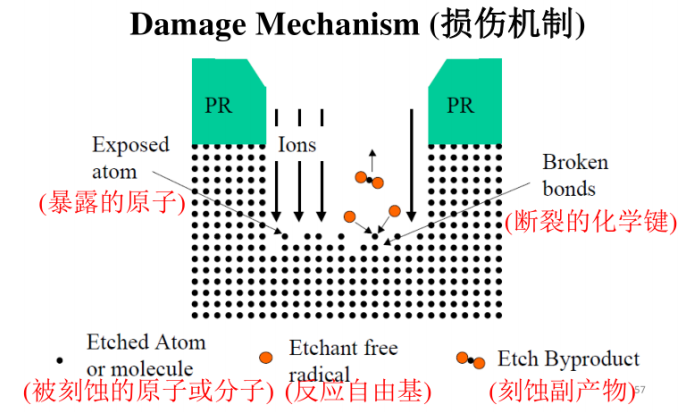
For the damage mechanism, strong ion bombardment breaks the chemical bonds between atoms on the wafer surface, and atoms with dangling bonds are acted upon by etching free radicals. These atoms readily form chemical bonds with free radicals from the etchant, resulting in volatile by-products that are removed from the surface. Since ion bombardment is perpendicular to the wafer surface, the etching rate in the vertical direction is much higher than in the horizontal direction, allowing plasma etching to form anisotropic etching profiles. Using the damage mechanism for etching is a process close to physical etching in RIE.
-
Blocking Mechanism:
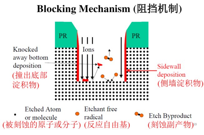
In the plasma etching process, ion bombardment can sputter some photoresist into the cavities. When photoresist is deposited on the sidewalls, it blocks etching in the sidewall direction, while photoresist deposited on the bottom will gradually be removed by ion bombardment from the plasma, exposing the bottom wafer surface to the etchant. Thus, this etching process is predominantly vertical.
This etching has long been used to develop various anisotropic etching technologies, such as the chemical deposits generated in anisotropic etching that protect the sidewalls and block horizontal etching. The ion bombardment required for etching using the blocking mechanism is less than that using the damage mechanism, thus achieving the goal of anisotropic etching.
Monocrystalline silicon etching, polycrystalline silicon etching, and metal etching generally adopt this mechanism, which is close to chemical etching in the RIE process. The sidewall deposits need to be treated through dry/wet cleaning or a combination of both cleaning methods.
Two types of anisotropic etching mechanisms and their simple applications in IC:
Recommended Books on Related Semiconductor Processes: