
Weighing Pros and Cons, Challenges and Adoption
Ashraf Takla, Mixel, Inc., CEO
Source: Mixel
(Originally published in April 2018. Updated in March 2022.)
MIPI® C-PHYSM was introduced in October 2014, generating both excitement and concern. How does this new C-PHY compare to MIPI D-PHYSM and M-PHY®? What are the differences with C-PHY, and is it compatible enough with D-PHY to coexist in a mixed subsystem?
Years later, the answers are clear.
This article will elucidate these answers, providing a high-level overview of D-PHY and C-PHY architectures, highlighting their similarities and differences, identifying the advantages and disadvantages of each PHY, and offering insights into some challenges encountered in implementing C-PHY. Finally, we will explore Mixel®’s innovative implementation of C-PHY/D-PHY combination IP, silicon results from multiple sources, cover use cases, and examine the market adoption of C-PHY/D-PHY combination solutions.
Let us first take a closer look at D-PHY, which has been around since 2009 and is therefore better understood and widely adopted. D-PHY is a simple source-synchronous PHY that uses one clock channel and a varying number of data channels. The block diagram of a D-PHY with four data channels is shown in Figure 1, with details of each channel illustrated in Figure 2. Due to D-PHY’s market presence for nearly a decade, there is a wealth of literature covering its unique features and use cases (1).
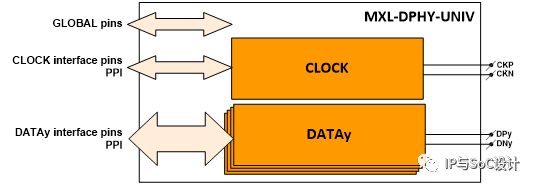
Figure 1: D-PHY Block Diagram with Four Data Channels
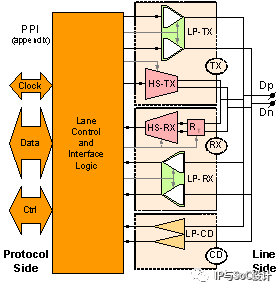
Figure 2: Block Diagram of D-PHY Data Channel
In contrast, C-PHY is a newer and more complex PHY. It operates on three signals in a three-in-one manner, with the clock embedded in the data, eliminating the need for a separate clock channel. The block diagram of C-PHY is shown in Figure 3.
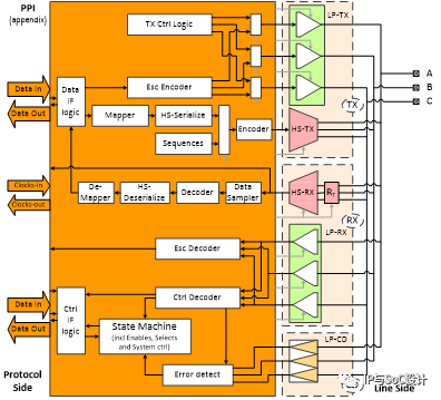
Figure 3: C-PHY Block Diagram
Table 1 compares D-PHY and C-PHY.
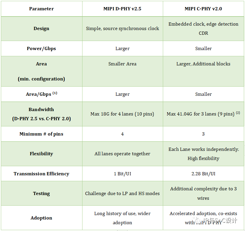
Table 1: C-PHY vs. D-PHY Parameters Comparison
Notes:
(1) Four data D-PHY channels versus three MIPI C-PHY channels
(2) Higher bandwidth due to encoding
C-PHY uses encoded data to pack 16/7≈2.28 bits/symbol, whereas D-PHY does not use any encoding. As a result, C-PHY can achieve higher data rates compared to D-PHY while operating at the same transition or symbol rate.
At first glance, the workings of C-PHY, and the potential C-PHY/D-PHY combination seem mysterious. C-PHY signaling is multi-level, but its receivers do not need to detect the differences between the levels! How is that possible? Why are there significant differences between C-PHY and D-PHY, yet they can not only coexist but also effectively combine into one IP? D-PHY uses differential signaling, while C-PHY employs triple signaling. Is it possible for them to work together? How can the C-PHY/D-PHY combination be effectively implemented using all D-PHY building blocks without any duplication? How is the ratio of 16/7 derived for the number of data bits per symbol? There are many questions to ponder!
Let us attempt to answer these questions, starting by unveiling the mystery of C-PHY. This is not an easy task. In Figure 4 below, we provide a quick overview of C-PHY. The block diagram in Figure 4(a) shows how a three-channel C-PHY TX and RX are connected. Figure 4(b) illustrates the different sub-blocks in the C-PHY subsystem, namely mapping, parallel/serial functions, encoding, and channels. Figure 4(c) provides a more detailed view of the interaction between TX and RX, and Figure 4(d) illustrates the signaling levels of C-PHY.
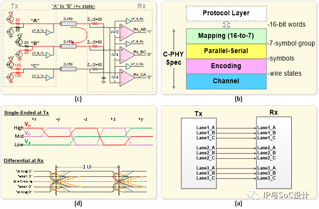
Figure 4: C-PHY (a) TX and RX Connections, (b) Different Functions in C-PHY Subsystem, (c) Detailed TX and RX Interaction, (d) C-PHY Signal Levels between TX and RX Outputs
A C-PHY lane consists of three components: A, B, and C, as shown in Figure 4(c). The C-PHY receiver comprises three differential RXs, each observing two of the three signals, namely (A-B), (B-C), and (C-A).
The C-PHY encoder ensures that (i) each symbol has at least one edge/transitions, (ii) all three RXs have non-zero differential inputs, and (iii) the common mode of all three signals is constant. The items (ii) and (iii) above are achieved by constraining the TX signals’ combinations within any single unit interval (UI) to high, mid, low, while keeping the voltage levels of each of the three signals different. The combinations of the three TX signal levels that meet the above constraint (i) can yield six different signal level combinations (line states). The number of line states, 6, is the permutation of the three TX signal levels, 3!. Additionally, the C-PHY encoder will flip, rotate, and polarity encode the state changes based on encoder rules.
To ensure that each symbol has at least one edge, as stated in item (i), C-PHY must transition between different line states when moving from one symbol to the next, and must not maintain the same line state in two consecutive symbols. Due to this constraint, there are five distinct unique transitions between the six line states. This means that the encoded data has five different possibilities, i.e., each symbol has five potential states, making C-PHY a quinary or quaternary system. Thus, we move between binary and quaternary systems. This is why a C-PHY mapper is needed. Now, we are using a quinary system, and the maximum theoretical number of bits/symbol is log2(5) = 2.3219. The construction of the mapper function is intended to make the mapping rate as close to but not exceeding this theoretical limit. Furthermore, the mapper must map between two integers. The choice of the ratio 16/7≈2.28 is made to achieve the above constraints.
Another way to describe this is that the mapper needs to map 16 binary bits to a certain number of C-PHY symbols, but how do we determine how many symbols (S) to map to? There are 2^16 combinations on the parallel interface, and the combinations at the mapper output are 5^S => 2^16, so S = 7.
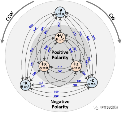
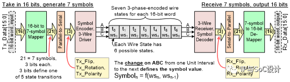
Figure 5: Overview of C-PHY Encoding and Mapping Functions
To understand why the C-PHY receiver only needs to detect the polarity of the input signals and not the amplitudes of multi-level signaling, we just need to remember that there is no data embedded in the signal amplitude. Multi-level signaling is only used to increase the number of possible transitions and ensure that each symbol has at least one transition.
A way to compare the performance of C-PHY and D-PHY is to compare them when they support a total data rate of 4.0Gbps and operate at similar transition rates. For D-PHY, this can be achieved using a four-channel D-PHY with ten data lines, each channel operating at 1.0Gbps/channel. To achieve the same or lower transition rate total data rate as C-PHY, we can use a dual-channel C-PHY with six lines operating at 0.875Gsps, which is lower than D-PHY’s 1.0Gsps. In this case, the total data rate for C-PHY is 2 * 0.875 * 16/7 = 4Gbps. This comparison is illustrated in Figure 6 below.
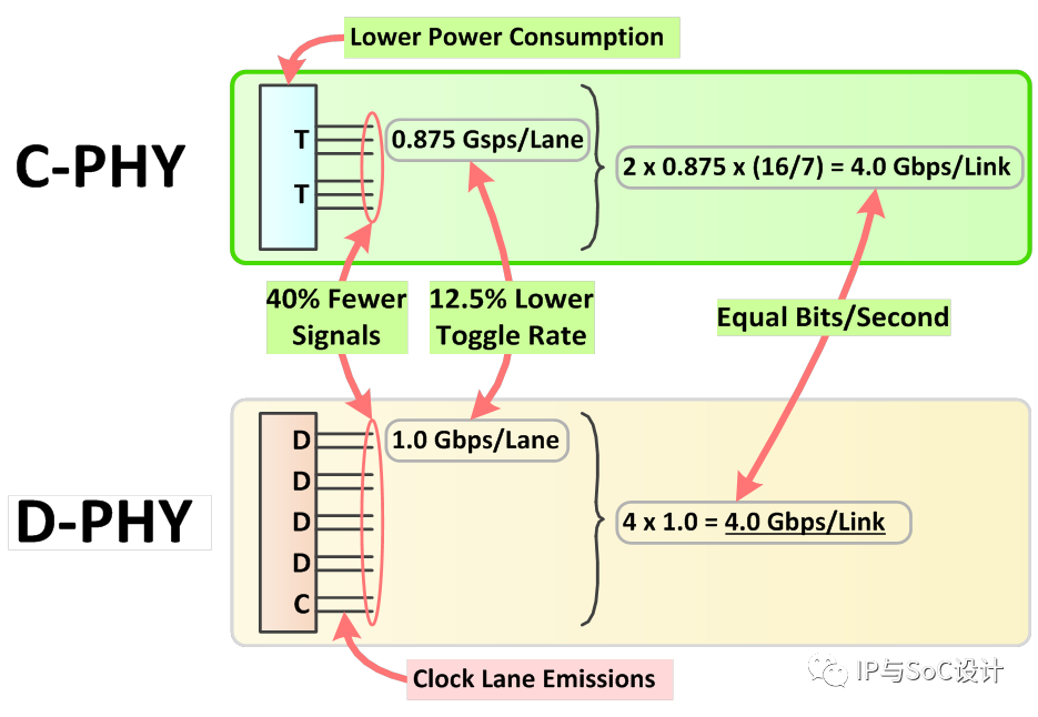
Figure 6: Comparison between D-PHY and C-PHY Supporting 4Gbps Aggregate Data Rate and Using Same Transition Rate
Based on this comparison, C-PHY has fewer wires (up to 40% less), lower switching rates/channel (12.5% lower), lower power consumption (approximately 20-50% lower), fewer channels, and thus a smaller area for the same Gbps without the consumption of a clock channel.
Therefore, when comparing C-PHY and D-PHY at the same total data rate, C-PHY has many advantages; fewer pins and balls (due to higher performance per pin), flexibility as each C-PHY channel is independent with an embedded clock that allows borrowing one channel from one link to another while coexisting with MIPI D-PHY on the same pins. C-PHY also allows for lower power in higher data rate applications. Furthermore, the embedded clock channel of C-PHY can allocate any channel on the application processor to any link and eliminates clock spurious emissions, which is particularly important in multi-band wireless devices.
The embedded control code of C-PHY also efficiently supports emerging features such as fast bus turnaround (BTA) operations, low latency (LRTE) for time-sensitive links, and backup low-power mode (ALP), which will achieve longer transmission distances by eliminating single-ended LP modes, thus reducing area. Finally, the lower switching rates of C-PHY generally simplify manufacturing and reduce costs for low-cost products such as entry-level cameras.
Now that we have understood the various attributes of C-PHY and D-PHY, we can enumerate some advantages of the C-PHY and D-PHY combination. These include the ability to share serial interface pins, reuse LP (low power) modes, and share common blocks, thereby reducing area and power/Gbps, achieving a smooth transition between MIPI D-PHY and MIPI C-PHY while leveraging the power/performance/area (PPA) improvements of MIPI C-PHY while maintaining compatibility with MIPI D-PHY.
Mixel’s implementation of C-PHY/D-PHY combination IP is unique. All D-PHY blocks are repurposed for C-PHY operation (HS-TX, HS-RX, SER, DESER, LP-TX, LP-RX, and LP-CD), minimizing the area overhead to support C-PHY. While all blocks are reused, additional modules required for C-PHY functionality include the encoder, decoder, CDR, mapper, and demapper. The block diagram of Mixel’s implementation is shown in Figure 7.
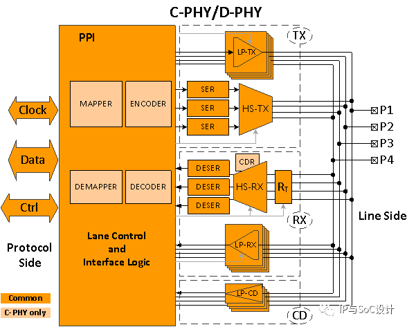
Figure 7: C-PHY/D-PHY Combination IP Block Diagram
Combo C-PHY/D-PHY has been implemented by Mixel across many different nodes and foundries. In fact, Mixel’s MIPI IP has been silicon-validated across 12 different nodes and 8 different foundries.
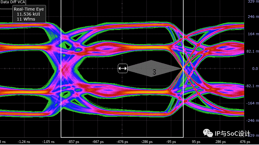
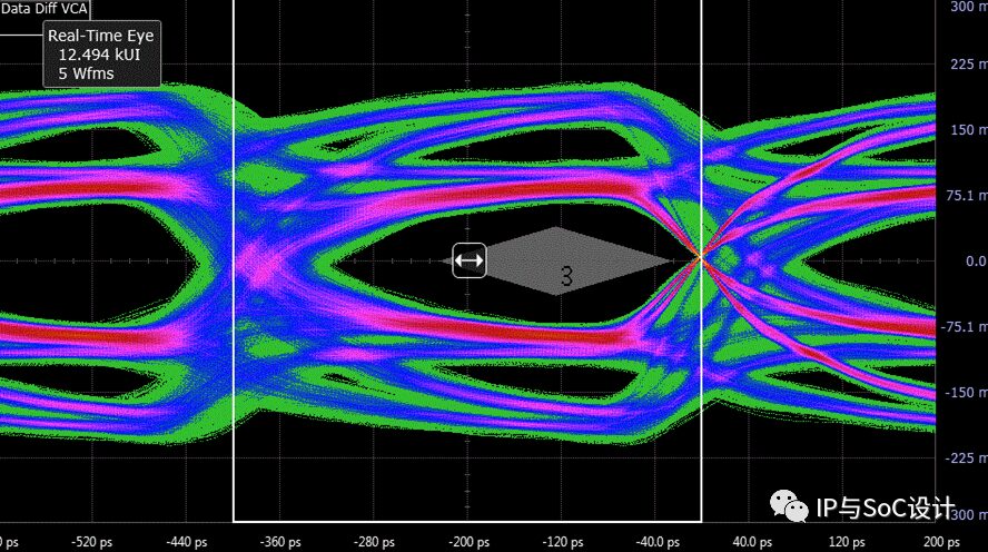
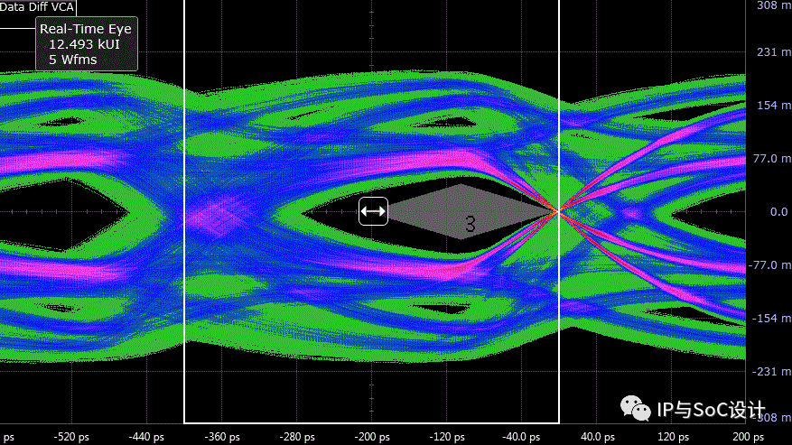
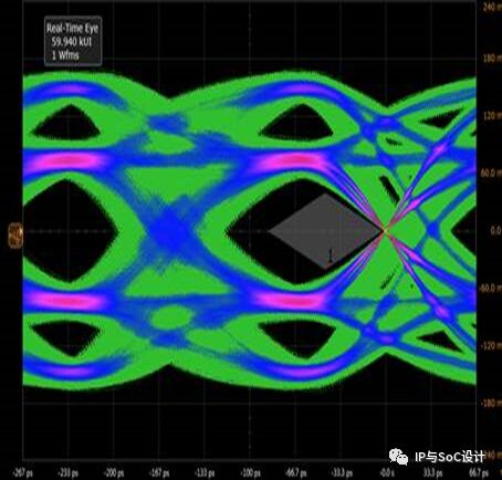
Below we showcase the test setups and chip evaluations for C-PHY and D-PHY transmitters.
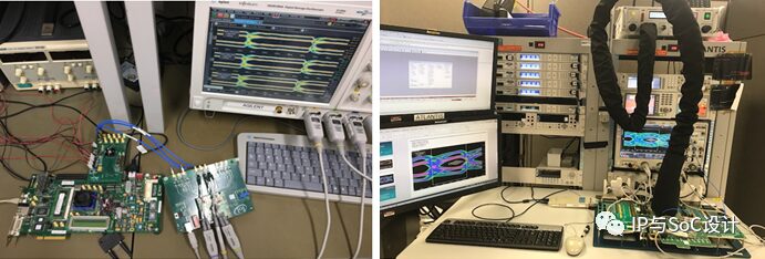
Figure 8: MIPI C-PHY Transmitter Test Setup
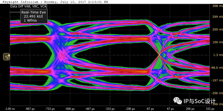
1.5Gsps
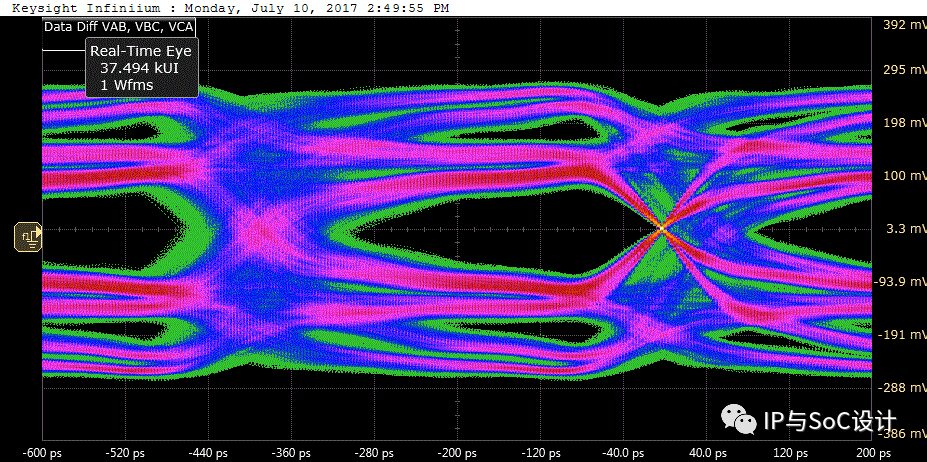
2.5Gsps
Figure 9: Chip Results: TX MIPI C-PHY – Eye Diagram (Mixel)
1.05Gsps @ std channel
2.5Gsps @ short channel
2.5Gsps @ std channel
Figure 10: Chip Results: TX MIPI C-PHY – Eye Diagram (Qualcomm)
3.5Gsps @ standard channel

2.5Gbps @ short channel
Figure 12: Chip Results: TX MIPI D-PHY – Eye Diagram (Mixel)
2.5Gbps @ short channel
4.5Gbps @ short channel
Figure 13: Chip Results: TX MIPI D-PHY – Eye Diagram (Qualcomm)
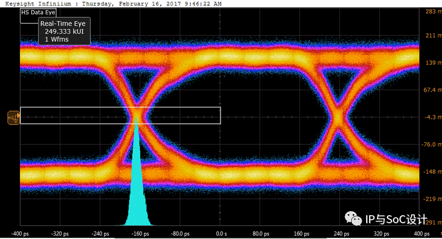
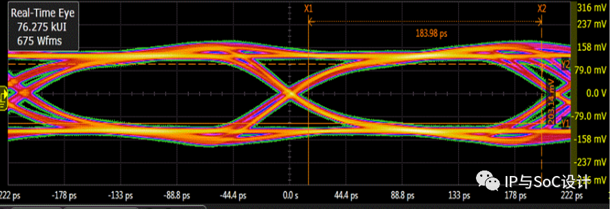
Below we showcase the test setups and silicon evaluations for C-PHY and D-PHY receivers.
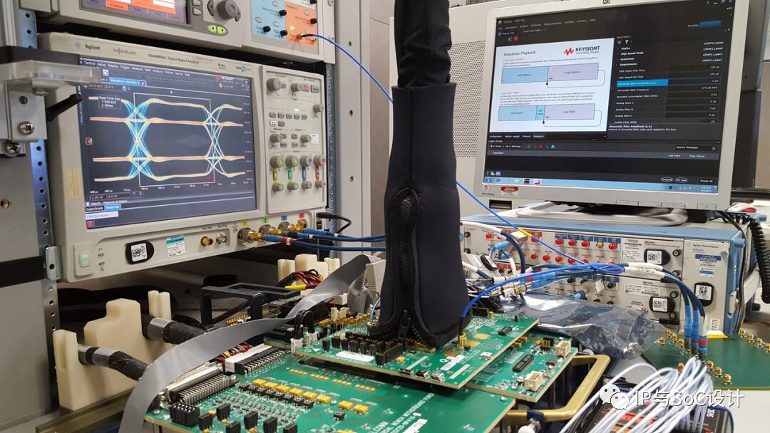
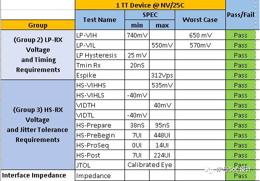
Figure 14: Chip Results: RX MIPI C-PHY – Electrical (Qualcomm)

Figure 15: Chip Results: RX MIPI C-PHY – Link (Qualcomm)
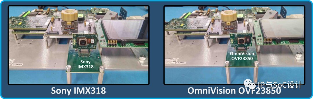
Figure 16: Example Use Case: Camera Invocation
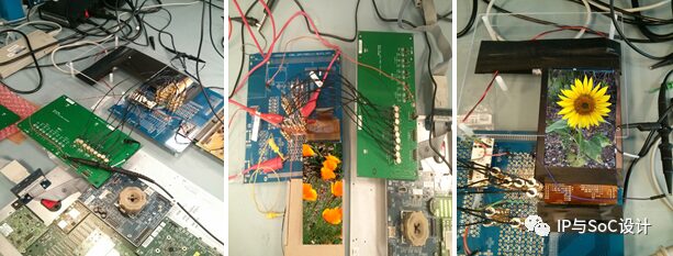
Figure 17: Example Use Case: Display Invocation
Now, let us look at the power, performance, and area for different use cases in current display and camera applications. These are shown in Table 3.
When comparing D-PHY and C-PHY/D-PHY combinations at the same data rates, the area increase is minimal. The normalized power of the C-PHY module alone is quite comparable when compared at the same Gbps. At the same transition rates, C-PHY has a significant advantage over D-PHY in achieving higher data rates.
However, the power increment of the combination PHY can be canceled by enabling multiple design options in the C-PHY mode configuration (not shown here).
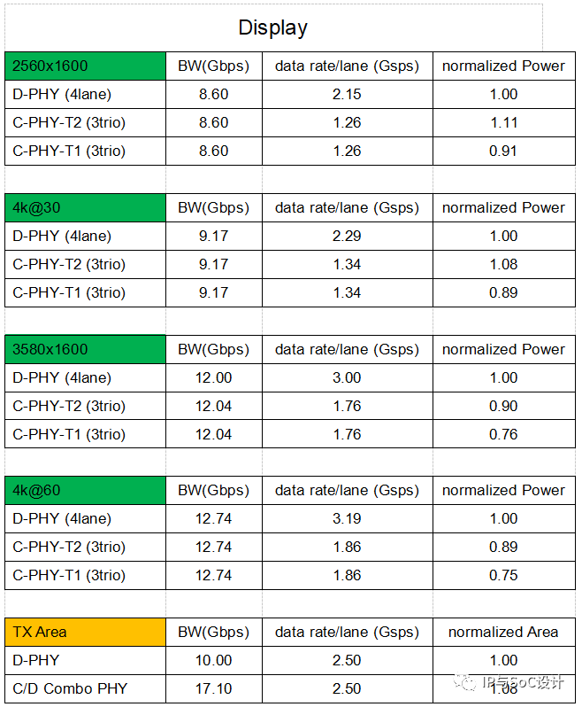
Table 3: PPA of Different Use-Cases for Display Applications
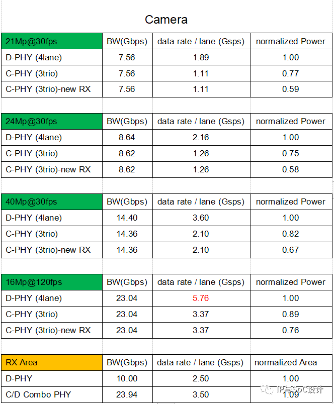
Table 4: PPA of Different Use-Cases for Camera Applications
Notes:
1. Combo PHY area increment < 10%
2. Combo PHY can cover a wide range of resolutions: 80Mbps – 10Gbps – 17.1Gbps – 18Gbps – 23.94Gbps
3. MIPI C-PHY Mode: Due to lower frequency/smaller offset/fewer channels, power consumption is about 10-30% lower than DPHY mode
4. Provided by Qualcomm
C-PHY/D-PHY combinations have been widely adopted across multiple use cases, many different vendors, and various types of products, including cameras (Sony, OVT, and others), displays (interoperability testing completed with most major DDIC companies). The ecosystem is supported by wide participation, including IP (Mixel), AP/SOC (Snapdragon, etc.), test equipment (Keysight, Tektronix, Introspect, The Moving Pixel Company), and common-mode filters (Murata, Panasonic, TDK).
However, the higher performance of C-PHY does not come without challenges; C-PHY presents some challenges, including the need for unique CDRs programmed for different data rate ranges, the introduction of encoded jitter from multi-level signaling, and the unique trio-based signaling that complicates PCB design.
In summary, MIPI C-PHY is a more complex, powerful, and efficient PHY, and the C-PHY/D-PHY combination is even more so. Mixel has created and silicon-validated dual-mode MIPI D-PHY/MIPI C-PHY, achieving a smooth transition between the two PHYs. Mixel’s dual-mode MIPI D-PHY/MIPI C-PHY shares all common modules, thereby reducing area and lowering power/Gbps. It offers the advantages of MIPI C-PHY PPA improvements while maintaining compatibility with MIPI D-PHY and using the same serial interface pins. Furthermore, the MIPI C-PHY/MIPI D-PHY combination has been silicon-validated across multiple nodes and foundries and has been integrated by many Tier 1 SOC, sensor, and display vendors into several end products. Since its debut, we have seen the MIPI C-PHY/MIPI D-PHY combination increasingly appealing for various applications in cameras and displays, including mobile and mobile-adjacent applications such as VR/AR/MR, automotive, IoT, etc.
This article reflects the author’s views only and does not represent the platform’s views.
If there are any disputes, please feel free to contact us.
If there is any infringement, please contact us for removal.