How difficult is it to achieve a complete “cradle-to-grave-to-cradle” cycle for electronic devices? A smartphone contains hundreds of materials, many of which are permanently bonded and encapsulated, making separation costly and prone to cross-contamination; moreover, components like chips are extremely sensitive to impurities, and any contamination in recycled materials can render them useless.

How can we ensure that materials do not lose performance during recycling and can be transformed back into clean raw materials? The team from the Chinese Academy of Sciences has made a significant step in this direction.
01
First, break down the base materials
Recently, a team led by Academician Yu Shuhong from the University of Science and Technology of China developed a “cellulose-based dielectric film” that can be recycled in a closed loop, significantly improving the recycling rate of electronic devices and reducing electronic waste pollution.
First, let’s explain what a “dielectric film” is; you can think of it as the “film” of a circuit. It is not conductive copper foil, but rather the layer that lies beneath the conductive patterns, separating the circuits.
Using a city road analogy, the metal traces in electronic products are like lanes leading in all directions, while the dielectric film acts as the “roadbed”. It must provide mechanical support, maintain road flatness and dimensional stability, while also separating different “lanes” to prevent collisions.
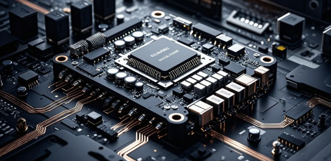
In electronic products, the dielectric film must prevent erratic current flow, withstand heat from chips, and endure various mechanical flexing—because it is used in various flexible screens.
Typically, the metal traces in electronic devices are made from high-purity metals, such as silver and cobalt. If these metals can be recycled with high purity, they can be transformed into sputtering targets for reuse in chip manufacturing.
Unfortunately, these metals have always been difficult to recycle because disassembling them from the dielectric film without any impurities is quite troublesome and not cost-effective.
However, what if there were a type of “dielectric film” that could be precisely decomposed, allowing the circuit metal traces to return on their own?
02
A special “sandwich” bio-based material
Traditional dielectric film substrates are difficult to separate into layers; they are usually physically recycled, which merely grinds the plastic substrate, leaving electronic components to be landfilled.
The research team in China drew inspiration from kombucha: could this bacteria grow a special biological material as a substrate?
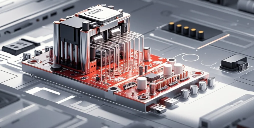
Without hesitation, they first allowed one of the key microorganisms in the fermentation of kombucha, “Acetobacter”, to be aerosolized and “parachuted” onto a nanocellulose mesh; these gel microspheres, which are only one-thousandth the diameter of a human hair, became the bacteria’s aerial “scaffolding”.
As the bacteria secreted cellulose strands, they spontaneously wove a “sandwich” structure—dense fiber layers on the top and bottom, with a cushioning layer filled with air microspheres in the middle.
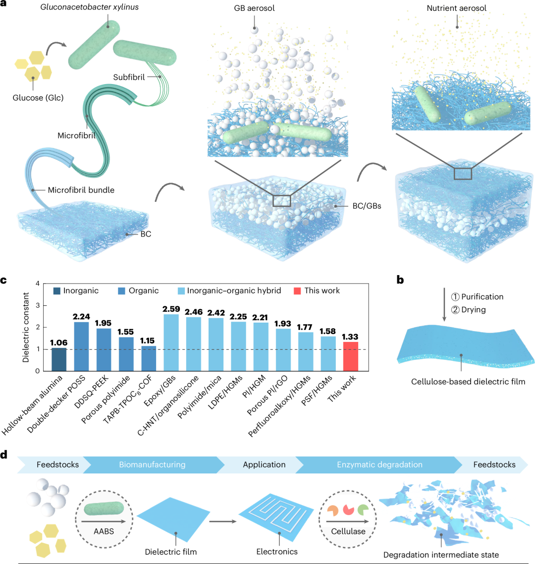
In other words, the dielectric film created by the research team is no longer a simple layer of material, but a three-layer structure. The outer two layers are plant fibers, like the two slices of bread in a sandwich, responsible for supporting the entire material and maintaining a flat, unwarped surface. The middle layer is not meat, but countless tiny “hollow spheres” filled mainly with air.
Why include these “spheres”? Because air is the least conductive. By evenly “sandwiching” a lot of air into the material, the electrical signals running across this “sandwich” will travel more smoothly with less loss, which is technically referred to as a lower dielectric constant.
At the same time, these spheres also provide structural support, making the sandwich structure lightweight and rigid, resistant to thermal expansion and contraction, and preventing the circuit drawn on it from cracking or deforming.
03
Gently disassembled with enzymes
The most obvious advantage of using cellulose is its recyclability. The research team found that when the discarded cellulose substrate is immersed in a custom enzyme solution, the material dissolves into a transparent viscous liquid, much like sugar cubes dissolving in water, which is completely different from traditional plastic recycling.
Most importantly, this special cellulose enzyme precisely “cuts” and disassembles the cellulose without damaging the metal circuits, and the recovered solution can be aerosolized and reconstituted for use as a dielectric film.
This is a molecular-level material renewal. The research team mentioned in their paper that if 10% of flexible circuits worldwide adopted this material, it could reduce oil consumption by 4 million tons and carbon emissions by 12 million tons annually.
Of course, this technology currently focuses only on the performance and recyclability of the circuit substrate and does not yet involve the complete disassembly of silicon chips and packaging materials. If one day all the materials in our smartphones are similar to this, perhaps at the end of their lifespan, they could return to the earth like any other form of life.
 Subscribe on WeChat
 Welcome to subscribe to the 2025 Computer News via postal channelsPostal Issue Number: 77-19Price: 8 yuan, Annual Price: 400 yuanEditor|Zhang YiChief Editor|Li KunEditor-in-Chief|Wu Xin“Contact for tips:cpcfan1874 (WeChat)Yilong Media:Documenting fresh technology and internet news, e-commerce life, cloud computing, ICT fields, consumer electronics, and business stories. Included in the full-text weekly of China National Knowledge Infrastructure; one of the top 100 Chinese science and technology newspapers; a member of the Weibo Million Fans Club in 2021; a quality technology content creator on Douyin in 2022.”