Once you understand the memory access path, you might wonder: what exactly are the read and write requests sent out by the processor? To clarify this, we need to introduce the bus. Below, I will discuss the ARM’s AXI/ACE bus protocols and the bus structures derived from them. These two protocols are widely used in mainstream mobile chipsets and are part of the fourth generation of the AMBA (Advanced Microcontroller Bus Architecture) standard.A simple bus consists of some address lines and data lines, plus an arbiter, which can send the read and write requests from the processor to memory or peripherals and return data. In this process, we need a master device and a slave device; all transfers are initiated by the master, with the slave responding. Let’s consider the processor and its cache as the master device, while the memory controller acts as the slave device. The processor initiates an access request; if it is a read, the bus sends this request (including the address) to the memory controller and then waits for a response. After some time, the memory controller hands over the data read from the memory chip to the bus, which then delivers the data to the processor. If the data is correct (no ECC or parity errors), the read operation is complete. If it is a write, the processor sends the write request (including the address) and data to the bus, which passes it to the memory controller. After the memory controller completes the write, it provides an acknowledgment, which is sent back to the processor via the bus, completing the write operation.There are several key points in the above process. First, a single read instruction in the processor is divided into a request (address) and a completion (data) phase. The write instruction is also divided into request (address, data) and completion (write acknowledgment) phases. Second, as the slave device, the memory controller can never actively initiate read or write operations. If it needs to communicate with the processor, for example, due to a read or write error, it must use an interrupt to prompt the processor to initiate a request to read the status of the memory controller. Third, incomplete read and write instructions become outstanding transactions (OT), and the bus can support multiple OTs. However, just because the bus supports multiple OTs does not mean the processor can send out that many requests, especially for reads. Therefore, the bottleneck may still lie with the processor.I have encountered situations where, while running a certain driver, the system suddenly hangs. However, other device interrupts can still respond, or after reporting an exception, the system continues running. If we replace the memory controller mentioned above with a device controller, it becomes easier to understand this phenomenon. Suppose the processor initiates a read request to the device, but the device does not respond; the processor will wait indefinitely. The processors I have seen, including PowerPC and ARM, do not have a timeout mechanism for such situations. Without an interrupt, the processor cannot switch to another thread (in exclusive mode in operating systems like Linux) and will keep waiting, causing the system to appear to be hung. Some device controllers can automatically detect such timeouts and call the corresponding exception or interrupt handler through an interrupt. In the interrupt handler, an error can be reported, the return address can be modified, and the execution can skip the previous instruction to continue, allowing the system to recover. Some processors can automatically jump to the next instruction after triggering a certain type of exception to avoid hanging. However, if no exception or interrupt occurs, it will hang indefinitely.Returning to the bus, in the AXI/ACE bus protocol, read and write operations are separated into different channels because there is no inherent connection between them. More specifically, the bus defines five groups: read operation address (master to slave), read operation data (slave to master), write operation address (master to slave), write operation data (master to slave), and write operation acknowledgment (slave to master). There is no specified order between the two major types of operations, read and write. However, within each type of operation, there is a specified order among the groups; for example, the address is sent first, followed by the data, which can have multiple cycles, forming burst operations. The acknowledgment in write operations is given after the slave device receives the data. For the memory controller, it must provide acknowledgment only after the data has been finally written to the chip, not just when the data is received and placed in internal buffers.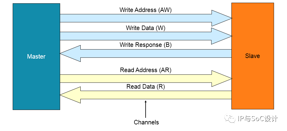 For the same channel, if consecutive instructions are received, what is their order? The AXI/ACE protocol stipulates that the order can be scrambled. Taking reads as an example, the data returned for two consecutive read instructions can be out of order. This raises the question of how the bus distinguishes between the two read instructions. It is simple; by adding several signals to the address and data groups as identifiers to differentiate between read requests and completions numbered 0-N. Each pair of requests and completions uses the same identifier. With this identifier, there is no need to wait for the previous request to complete before starting the second request; instead, they can be processed alternately, thus achieving bus OT and greatly improving efficiency. Of course, corresponding buffers must be provided to store the status of these requests. The maximum number of OTs is determined by the smaller of the number of buffers and identifiers. The reason is simple: if buffers or identifiers run out, but all read operations are requests with none completed, the new requests must wait. Hence, there is a rule in the AXI/ACE bus: requests with the same identifier in the same read or write channel must complete in order.Sometimes, the processor may also use this identifier as its internal read/write request identifier, as Cortex-A7 does. This is not ideal because it imposes a restriction on itself, limiting the maximum number of outstanding transactions to be no greater than the number of identifiers per bus channel. When there are four cores in a processor group, this limit may not be sufficient, artificially constraining the number of OTs.Finally, there is no specified order between read and write channels, even if they share the same identifier.At this point, you might have a question: in read and write instructions, there is a default principle that if the same address or overlapping addresses are accessed, memory access must be sequential. Additionally, if the type of memory being accessed is a device, the memory access order must be consistent with the instructions. How is this reflected on the bus? The bus checks the addresses to ensure order; generally, the addresses for out-of-order memory accesses cannot be within 64 bytes, and for device accesses, they cannot be within 4KB.In AXI/ACE, the ratio of read to write channels is one to one. In practice, the probability of reads is higher than that of writes. Of course, write caches are typically accompanied by cache line fill (read), while read caches can cause cache line eviction (write), along with merging and reordering, so the ratio of read to write instructions is not always straightforward. I have seen that the Freescale PowerPC bus CCB has a read to write channel ratio of two to one. I do not know why ARM did not design a similar approach to improve efficiency; perhaps one to one is based on the best ratio derived from typical mobile application statistics.Thus, we can now imagine the transmission situation of read and write operations in a pair of read and write channels. What happens when multiple master and slave devices are combined? Is it simply an addition? This involves the core issue of bus design: topology.In ARM’s current bus products, based on different topologies, they can be classified into three categories: NIC/CCI series is crossbar (Crossbar), CCN series is ring-based (Ring), and NoC series is mesh-based (Mesh). Each has its characteristics and is suitable for different scenarios. The number of master and slave devices connected by a crossbar is limited, but it is the most efficient; read and write requests can reach the slave device in 1 to 2 cycles. As shown in the figure below, this is a 5×4 crossbar:
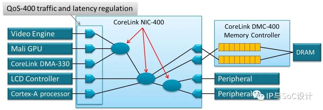 According to the data I have seen, on a 28nm process, under a 5×4 configuration, this bus can run at a frequency of 300MHz. If the number of master and slave pairs is further increased, due to increased fan-out, capacitance, and routing, more registers must be inserted to increase the frequency. However, this will also increase the delay from master to slave. Even maintaining a 5×3 configuration, to further increase to 500MHz, either better processes must be used (I have seen 800MHz on 16nm), or 2-3 levels of registers must be inserted, resulting in read/write delays reaching 4-5 bus clock cycles, with a total of 10 cycles for requests and completions. If the bus and processor frequency ratio is 1:2, then the time spent merely on the bus requires at least 20 processor clock cycles. With a ratio of 4, the time extends to 40 clock cycles. It is worth noting that the delay for processor access to the second-level cache typically does not exceed a dozen processor cycles. Of course, increasing the number of OTs can reduce average latency, but due to the limited number of OTs for the processor, especially for sequential processors, it may only be 1-2. Therefore, to achieve higher frequencies and support more master and slave devices, the CCN series ring bus must be introduced, as shown in the figure below:
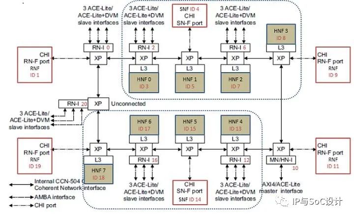 Each node on the CCN bus can communicate with its two adjacent nodes and can also connect two additional node components, such as processor groups, level-three caches, memory controllers, etc. Within the node, the connections are still crossbar, while between nodes, they are ring-based. This allows the bus frequency to be somewhat freed from the limitations of the number of connected devices (though still affected by routing and other factors) and can exceed 1.2GHz at 16nm. However, the trade-off is a greater average delay in inter-node communication. To reduce average latency, frequently accessed nodes can be placed closer together.In some systems, there is a requirement to connect more devices and achieve higher frequencies. At this point, the ring bus is not sufficient. The NoC must step in, as shown in the figure below:
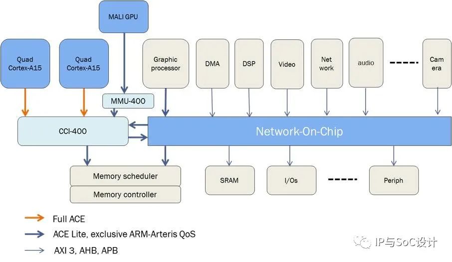 In this diagram, the previously mentioned crossbar can serve as part of the entire network. The nodes located within the NoC connect the entire system. Each node is a small router, and the data transmitted between them is asynchronous packets. This eliminates the need to maintain a large number of connections between routers, thus increasing frequency and supporting more devices. However, the downside is a longer delay. Based on the data I have seen, on 16nm, the frequency can reach 1.5GHz. Moreover, the frequency and topology structure between each submodule connected can differ. Devices that need to be closely linked, such as CPU clusters and GPUs, can be placed within the same subnet to reduce communication latency.You may have noticed that each of the bus types mentioned above has a prototype in network devices. From direct connections to devices to ring local area networks to switching and routing, their topological structures are interconnected.In the actual ARM ecosystem, how are these three topological structures used? Generally, crossbars are used in mobile chipsets, ring networks in network processors and servers, while mesh topology is also widely used in mobile chipsets. The latter is not due to the large number of devices needing to connect in mobile phones, but because the AXI/ACE protocol does not support splitting a single transmission into multiple parts to send to different memory controllers. This type of transmission is referred to as interleaving. Interleaving has many definitions; from the bus perspective, one is that the completion order of multiple read/write requests between a master device and a slave device can be scrambled, which we have already explained. The second definition is that for a single read/write request from a master device, it is sent to multiple slave devices, and completion is awaited. Why is this type of transmission necessary? Because in mobile phones, the GPU, display controller, and video controller have high memory bandwidth requirements. A 1080p screen requires refreshing 60 times per second, with 2 million pixels, each pixel having 32 bits of color, plus 8 layers, necessitating 4GB/s of data. However, a 1.6GHz transmission rate DDR3 controller with 64-bit data can only provide a theoretical bandwidth of 10GB/s. The theoretical bandwidth and actual bandwidth can differ significantly due to various factors, and achieving a 70% utilization rate is already commendable. So what about the processor and other controllers? The only solution is to increase the number of memory controllers, meaning adding more slave devices. However, simply increasing the number is not enough. The reason is that if different physical address requests are sent to different memory controllers, it is likely that at any given time, all physical addresses correspond to only one, which still cannot meet the bandwidth requirements. The solution is to split every address into multiple requests and send them to different memory controllers. Moreover, this task is best not handled by the processor (ARM cores do not support split reads/writes), as only the bus knows how many memory controllers there are. Ideally, the processor should only send requests, and the bus should handle all the splitting and collect the data before returning it to the processor.Unfortunately, the AXI/ACE bus naturally does not support one-to-many interleaving. The reason is simple: it can lead to deadlocks. Imagine two master devices and two slave devices connected via a crossbar. M1 sends two read requests, both with identifier 1, sent sequentially to S1 and S2, and waits for completion. Then M2 does the same, with identifier 2, sent to S2 and S1. At this point, if S2 finds that exchanging the return data would be more efficient, it does so. However, M1 cannot receive S2’s return data because, according to the rule that requests with the same identifier must complete in order, it must wait for S1’s return data. S1, meanwhile, cannot send data to M2 because M2 is also waiting for S2’s return data, resulting in a deadlock. The solution is that any master device cannot simultaneously send requests to multiple slave devices. Hence, multi-memory controller interleaving cannot be implemented.However, the mesh bus based on packet transmission does not have this issue; all packets are asynchronous, and there are no dependency relationships. Thus, a company specializing in NoC buses, Arteris, seized this opportunity to sell buses that support simultaneous access to multiple memory controllers to most companies producing mobile and tablet chipsets. As of now, ARM also has a solution, Arachne, but it has not seen much practical application.Currently, many mid-to-low-end mobile phones have 8 cores, and according to ARM’s design, there can be a maximum of four cores in each processor group. This necessitates placing two processor groups in the system, and the communication between them, including the implementation of big.LITTLE cores, requires bus coherence. Each processor group also needs coherence internally, and the principles are the same as external coherence, so I will not explain it separately. Software can achieve coherence, but that requires manually flushing the cache contents to the next level cache or memory. For a 64-byte cache line with a 64KB cache, this would require 1000 flushes. Assuming each takes 100 nanoseconds, and with OT=4, that would take 25 microseconds. This is a very long time for a processor. ARM has introduced a coprocessor to handle this, which is one solution. To solve it with hardware, ARM has introduced several buses that support hardware coherence; the following diagram shows the first generation solution, CCI400:
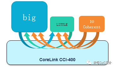 How does CCI400 achieve hardware coherence? Simply put, processor group C1 sends a special read/write command containing address information to the bus, and then the bus forwards this command to another processor group C2. Upon receiving the request, C2 progressively checks its level-two and level-one caches based on the address. If it finds that it has the data, it returns the data or performs the corresponding cache coherence operation, a process known as snooping. I will not elaborate on specific operations; ARM uses the MOESI coherence protocol, which defines all of this. In this process, the requesting core in C2 does not participate; all work is done by the cache and bus interface unit (BIU) and other components. To comply with the definition that slave devices do not actively initiate requests, two sets of master-slave devices are required, with each processor group occupying one master and one slave. This allows the two processor groups to maintain coherence with each other. Some devices, like DMA controllers, do not have caches and do not require snooping, so they only contain slave devices, as shown in the orange part of the above diagram. In ARM’s definition, interfaces with bidirectional functionality are called ACE, while those that can only snoop are called ACE-Lite. They not only have the read and write channels of AXI but also include a snooping channel, as shown in the following diagram:
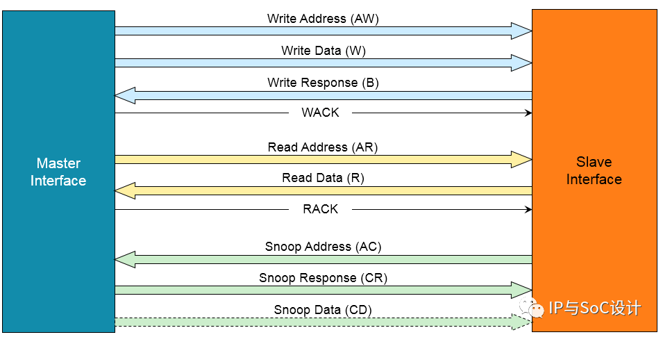 The additional snooping channel also has address (slave to master), response (master to slave), and data (master to slave) lines. Each group of signals contains identifiers similar to AXI to support multiple OTs. If data is found in the master device (a hit), the data channel will be used; if not, it simply informs the slave device of the miss without needing to transmit data. Thus, for the aforementioned DMA controller, it will never transmit data to others, so it does not require a data group, which is the main difference between ACE and ACE-Lite.We can also see that there is an additional line, RACK, on the read channel. Its purpose is that when the slave device sends data during a read operation to the master, it does not know when the master will receive this data because, as mentioned before, inserting registers can increase bus delay. If at this moment it needs to send a new snooping request to the master for the same address A, a problem arises: has the master already received the data sent for the previous address A? If it has not received it, it might inform the snooping that it is a miss. However, in reality, the data for address A has already been sent to the master, and it should return a hit. With the addition of RACK, the slave device will not send a new snooping request to the master until it receives the acknowledgment RACK from the master, thus avoiding the aforementioned issue. The WACK on the write channel functions similarly.We previously calculated the delay on NIC400; with the hardware synchronization of CCI400, does this mean access is faster? First, the purpose of hardware coherence design is not to be faster but to simplify software. In reality, it may not necessarily be faster. Because given an address, we do not know if it is in the cache of another processor group, so additional snooping actions are always required. When there is a miss, this snooping action is redundant because we still need to fetch data from memory. This unnecessary action introduces additional delay, totaling 10 plus 10, which equals 20 bus cycles, representing a 100% increase. Of course, if there is a hit, although the total bus time still requires 10 cycles, fetching data from the cache is faster than fetching from memory, thus providing benefits at that time. Overall, when the hit rate exceeds a certain percentage, the overall performance still benefits.However, from the perspective of practical application programs, except for specially designed programs, the hit rate typically does not exceed 10%. Therefore, we must think of ways to improve performance. One method is to have the bus fetch data from memory regardless of whether the result is a hit or a miss. When the data is retrieved, we also know the snooping result, allowing us to decide which data to send back. The downside of this approach is increased power consumption since it requires fetching from memory regardless. Secondly, when memory access is already frequent, this approach can reduce overall performance.Another method is that if we know in advance that the data is not in the cache of other processor groups, we can allow the master device issuing the read/write request to explicitly state that snooping is not needed, and the bus will skip this action. The downside of this method is that it requires software intervention; although the cost is not high (setting a register when allocating operating system pages), it raises the requirements on programmers, who must fully understand the target system.The designers of the CCI bus have also employed a new method to enhance performance. They have added a snooping filter to the bus. This is essentially a cache (TAG RAM) that contains the state information of all level-one and level-two caches within the processor groups. Data cache (DATA RAM) is unnecessary because it only needs to check for hits or misses. The benefit of this approach is that snooping requests do not need to be sent to each processor group; they can be completed within the bus, saving nearly 10 bus cycles, and the power consumption is lower than accessing memory. The downside is the addition of a small amount of cache (about 10% of level-one and level-two caches). Moreover, if a line in the snooping filter is replaced (for example, when a write snooping hits and requires invalidating a cache line, as defined by the MOESI protocol), the same operation must be performed in the corresponding level-one and level-two caches of the corresponding processor group to maintain coherence. This process is known as reverse invalidation, which adds an extra burden because the snooping filter must also track the updated status during updates to the level-one and level-two caches; otherwise, coherence cannot be guaranteed. Fortunately, actual testing has shown that such operations do not occur frequently, typically not exceeding 5%. Of course, some test codes may frequently trigger this operation, and at that point, the downsides of the snooping filter become apparent.The ideas above are implemented in CCI500, as illustrated in the following diagram:
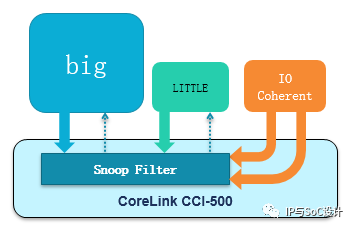 After actual performance testing, the designers of CCI found that the bus bottleneck shifted to accessing this snooping filter window. This bottleneck actually masked the earlier mentioned reverse invalidation issue, as it was always discovered before reverse invalidation. After widening this window, testing showed that if every master-slave interface were to push data aggressively (with unlimited OT for both master and slave devices, and with multiple masters sending requests to multiple slaves), there would often be waiting situations at the master-slave device interfaces. This means that even though data is ready, the devices cannot keep up with receiving it. Therefore, additional buffers were added to store this data. The cost is slightly larger area and power consumption. Note that this buffer does not duplicate the buffer that stores OT status.According to empirical data, after implementing all the improvements, the new bus bandwidth performance has increased by over 50% at the same frequency. The frequency can increase from 500MHz to 800MHz. Of course, this result is just a rough statistic; if we consider the limited number of OTs for the processor and the variable hit rates of the data being snooped, we will definitely get different results.As a bus used in mobile chipsets, it needs to support multiple priorities for transmission, which is QoS. This is because devices like display controllers have high real-time requirements, and requests from processor groups are also important. Supporting QoS itself is not difficult; it only requires placing various requests in a buffer and transmitting them based on priority. However, in practical tests, it was found that if the requests from various devices are too numerous and frequent, the buffer quickly fills up, blocking new high-priority requests. To solve this problem, the buffers were grouped according to priority, allowing each group to only accept requests of equal or higher priority, thus avoiding blocking. These methods are similar to network congestion control designs.Furthermore, to support multiple clock and power domains, allowing each processor group to dynamically adjust voltage and clock frequency, the CCI series buses can also be paired with asynchronous domain bridges (ADB). This has a certain impact on performance; when the frequency ratio is 2, signals passing through it require an additional bus clock cycle. If it is 3, it is even longer. In systems with strict access latency requirements, this time cannot be ignored. If there is no need for additional power domains, we can skip it to save some latency. The NIC/CCI/CCN/NoC buses inherently support asynchronous transmission.Related to coherence are memory access orders and locks; some programmers confuse them. Suppose we have two cores, C0 and C1. Whenever C0 and C1 access the same address A0, it must be ensured that the data they see is consistent; this is coherence. Then, within C0, it needs to ensure that accesses to addresses A0 and A1 occur in order, which is referred to as access order. This does not require locks, only barrier instructions. If C0 and C1 are running two threads simultaneously, and both access the same address A0 and need to ensure that C0 and C1 access A0 in order, this requires locks. Therefore, barrier instructions can only guarantee single-core, single-thread order; multi-core, multi-thread order requires locks. Coherence ensures that when performing lock operations, different copies of the same variable in caches or memory are consistent.ARM’s barrier instructions are divided into strong barriers (DSB) and weak barriers (DMB). We know that read and write instructions are divided into request and completion phases. Strong barriers require that the previous read or write instruction completes before the next request can start, while weak barriers only require that the previous read or write instruction has been issued before proceeding with the next request, and it can only guarantee that when the subsequent read and write instructions are completed, the previous read and write instructions must have been completed. Clearly, the latter situation has better performance, with OT>1. However, tests show that in cases with multiple processor groups, when barrier instructions are transmitted to the bus, the overall system performance can only decrease; therefore, in the new ARM bus, barriers are not supported and must be handled by the processor itself at the chip design stage through configuration options, indicating to the processor to handle barrier instructions without sending them to the bus. However, this does not affect barrier instructions in the program, as the processor will filter them out before they reach the bus.Specifically, how is the barrier mechanism implemented on the CCI bus? First, barriers, like read and write instructions, also use the read and write channels, but their address is always 0 and there is no data. Identifiers are also present, along with two additional lines, BAR0/1, indicating whether this transmission is a barrier and what type of barrier it is. How is it transmitted? First, consider the weak barrier, as shown in the following diagram:
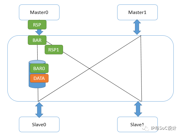 Master0 writes some data, then issues a weak barrier request. At the point where CCI and the master device interface receive the barrier request, they immediately do two things: first, send a barrier response to Master0; second, send the barrier request to the interfaces of slave devices Slave0/1. The Slave1 interface quickly gives a barrier response because there are no pending transmissions there. However, the Slave0 interface cannot give a barrier response because the data has not yet been sent to the slave; the barrier request must wait in this path and cannot swap order with the data write request. This does not prevent Master0 from issuing a second data write, as it has already received barrier responses from all its lower interfaces (Master0 interface), allowing it to write out the flag. As shown in the following diagram:
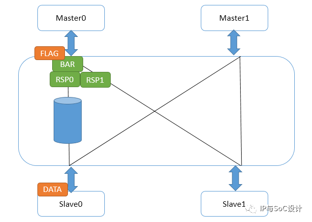 At this point, the flag waits at the Master0 interface for barrier responses from all its lower interfaces. Once the data reaches Slave0, the barrier response reaches the Master0 interface, and the flag continues to proceed. At this stage, we need not worry about the data not reaching Slave0 because, prior to that, the barrier response from Slave0 will not be sent to the Master0 interface. Thus, weak barrier order guarantees are achieved, and the flag request can be sent out before the barrier instruction is completed.For strong barrier instructions, the only difference is that the Master0 interface will not send its own barrier response to Master0 until it has received barrier responses from all lower interfaces. This prevents the flag from being sent out until the barrier instruction is completed. As shown in the following diagram:
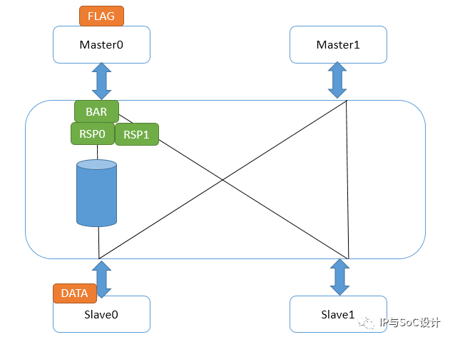 Thus, it is ensured that the next read/write instruction can only be issued after the strong barrier is completed. At this point, the read/write instructions preceding the strong barrier must have been completed.It is also important to note that ARM’s weak barriers only target explicit data access orders. What is explicit data access? Read/write instructions, cache, and TLB operations count. Conversely, what is implicit data access? In the processor section, we mentioned that processors have speculative execution, pre-executing read/write instructions; caches also have hardware prefetch mechanisms that automatically fetch cache lines likely to be used based on previous data access patterns. None of these are included in the current instructions, and weak barriers cannot affect them. Therefore, it is crucial to remember that weak barriers can only guarantee the order of the instructions you provide and cannot ensure that no other modules access memory between them, even if that module comes from the same core.In simple terms, if you only need to guarantee read/write order, use weak barriers; if you need to ensure that a certain read/write instruction completes before doing something else, use strong barriers. The above applies to ordinary memory types. When we set the type to devices, strong barriers are automatically guaranteed.We mentioned that barriers only apply to single-core scenarios. In multi-core, multi-thread scenarios, even with barrier instructions, atomicity of read/write operations cannot be guaranteed. There are two solutions: one is software locks, and the other is atomic operations. The atomic operation I have seen involves the bus receiving requests and directly blocking the entire bus, allowing only one core to access it. This is very inefficient. Another method is to send the lock request to the opposing device, such as the memory controller, to prohibit access from other cores while the bus continues to operate, which significantly improves efficiency. The data I have seen indicates a reduction in time by a factor of ten. However, the AXI/ACE protocol does not support atomic operations, so software locks are necessary.A software lock can be implemented using an ARM hardware mechanism called exclusive access. When a special instruction writes a value to an address, a special mark is placed on the corresponding cache line, indicating that no other core has written to this line. The next instruction reads this line; if the mark has not changed, it shows that there has been no interference between the write and read, thus acquiring the lock. If it has changed, it returns to the write process to re-acquire the lock. Due to cache coherence, this lock variable can be used by multiple cores and threads. Of course, barriers are still needed in the process to ensure order.For ordinary memory, there is also a problem: read/write operations may go through the cache, and you do not know whether the data has ultimately been written to memory. Typically, we use clean operations to flush the cache. However, flushing the cache is itself a vague concept; caches exist in multiple levels, some in the processor, some after the bus—where exactly does it need to be flushed to be considered complete? Additionally, to ensure coherence, does it need to notify other processors and caches during the flush? To standardize these issues, ARM introduced the concepts of Point of Unification/Coherency, Inner/Outer Cacheable, and System/Inner/Outer/Non-Shareable.
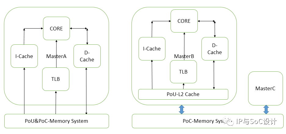 PoU refers to a point where, for a given core Master, the instructions, data caches, and TLB associated with it see consistent content at a specific point. In the illustration on the right, MasterB includes instructions, data caches, and TLB, as well as level-two cache. The data exchanges between instructions, data caches, and TLB are based on the level-two cache, making it the PoU. For MasterA on the left, since it does not have level-two cache, the exchanges occur in memory, making memory the PoU.PoC refers to a point in the system where all Masters (note that it is all, not just a specific core) can see the same source for their instruction, data caches, and TLB. In the illustration on the right, the level-two cache cannot serve as PoC because MasterB is outside its scope and directly accesses memory. Thus, memory serves as PoC at this point. In the left diagram, since there is only one Master, memory is PoC.Furthermore, if we replace the memory in the right diagram with level-three cache and connect memory after the level-three cache, then PoC will become the level-three cache.With these two definitions, we can specify the range of cache operations and read/write instructions. For example, in the following system diagram, there are two A15 groups, each containing four cores and level-two caches. The system’s PoC is in memory, while the PoU for both A15s is in their respective level-two caches. When executing a Clean instruction on a certain A15 and specifying the range as PoU, it is evident that all four A15s’ level-one instruction caches will be cleared. But will this affect other Masters? That will depend on the Inner/Outer/Non-Shareable settings.
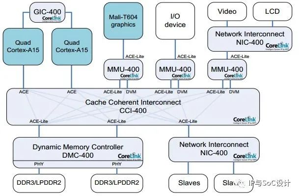 Shareable is easy to understand; it means that a certain address can potentially be used by others. We specify this when defining the properties of a certain page. Non-Shareable means it is only for self-use. However, defining something as Non-Shareable does not mean others cannot use it. If an address A is mapped as Shareable on core 1 and Non-Shareable on core 2, and the two cores are connected via CCI400, when core 1 accesses A, the bus will snoop core 2, while when core 2 accesses A, the bus will directly access memory without snooping core 1. This approach is clearly erroneous.For Inner and Outer Shareable, a simple understanding is that data sharing belongs to Outer Shareable; instruction and TLB sharing, which are read-only, belong to Inner Shareable and also qualify as Outer Shareable. In the system depicted in the above diagram, A15 and A7 share instructions, making them Inner Shareable. Of course, their data is also shared, thus qualifying as Outer Shareable. However, between DMA, Mali, and the processor, only data is shared, so it is not Inner Shareable but Outer Shareable.When integrating ARM processors like A15/A7 into SoC systems, we need to set the Inner and Outer Shareable attributes. Setting Inner means that instruction operations and read-only accesses to instruction caches and TLB will be sent to the bus. Setting Outer means that data operations and accesses to data caches will be sent to the bus. Moreover, if Outer is set, Inner must also be set. The reverse is not necessary. Normally, both should be set.After discussing so many concepts, you might wonder what their practical use is. Returning to the Clean instruction, PoU ensures that the corresponding lines in the instruction caches of the four A7s are cleared. Since it is an instruction cache operation, the Inner Shareable attribute allows this operation to be broadcasted to the bus. The CCI400 bus will broadcast this operation to all potentially receptive ports. The ACE port is the first to respond, so the corresponding instruction cache lines of the four A15s will also be cleared. For Mali and DMA controllers, which are ACE-Lite, they technically do not need to be cleared. However, note that they are still connected to the DVM interface, which is specifically responsible for receiving and sending cache maintenance instructions, so their corresponding instruction cache lines will also be cleared. However, in reality, they do not have corresponding instruction caches, so they merely accept requests without any actions.You might also wonder why we need such complex definitions. The purpose is to precisely define the scope of cache maintenance and read/write instructions. If we change things so that the bus does not support the broadcasting of Inner/Outer Shareable, then only the A7 processor group would clear the cache lines. Clearly, this is logically incorrect, as A7/A15 may run the same lines of code. Additionally, we previously mentioned that if we set the read/write attributes to Non-Shareable, the bus will not snoop other masters, thus reducing access latency, allowing for greater flexibility in improving performance.Returning to the earlier question of how to know whether data has ultimately been written to memory when flushing a certain cache line, I apologize, but unfortunately, we still cannot know. You can only set the range as PoC. If PoC is level-three cache, it will ultimately flush to level-three cache; if it is memory, it will flush to memory. However, this is logically sound; according to the definition, if all Masters see unified data in level-three cache, then there is no need to flush to memory.In summary, PoU/PoC defines the reach of instructions and commands to the caches or memory, and once they reach the specified location, Inner/Outer Shareable defines the scope of their broadcasting.Furthermore, consider Inner/Outer Cacheable, which is simply a definition of before-and-after cache. Level-one cache is always Inner Cacheable, while the outermost cache, such as level-three, can be either Outer Cacheable or Inner Cacheable. Their utility lies in defining different handling strategies for memory page attributes at different cache levels.In ARM’s processor and bus manuals, several Points of Serialization (PoS) will also appear. This means that in the bus, all types of requests from master devices must be checked by the controller for address and type; if there are conflicts, serialization will occur. This concept is unrelated to the other several.Looking at the entire evolution of the bus, there is a core issue that has not been mentioned: dynamic planning (re-scheduling) and merging. Both processors and memory controllers have similar modules responsible for classifying, merging, and adjusting the order of all transmissions, even predicting future read/write request addresses to achieve maximum transmission efficiency. This issue will be revisited when analyzing performance. Understanding the bus delay and maximum OT is beneficial for accurately matching the statistics from performance counters to see if expectations are met.Article source: https://www.zhihu.com/people/zhong-zou-ci-jian-luThe content of this article represents the author’s views and does not represent the platform’s views.If there are any objections, please feel free to contact us.