This series will introduce the basic knowledge of bare-metal programming with STM32 to better understand how frameworks and IDEs like STM32Cube and Keil work. This guide starts completely from scratch, requiring only a compiler and the chip’s datasheet, without relying on any other software tools or frameworks.
This series covers the following topics:
- Memory and Registers
- Interrupt Vector Table
- Startup Code
- Linker Script
- Using
makefor Automated Build - GPIO Peripherals and Blinking LED
- SysTick Timer
- UART Peripherals and Debug Output
- Redirecting
printfto UART - Debugging with Segger Ozone
- System Clock Configuration
- Implementing a Web Server with Device Dashboard
We will use the Nucleo-F429ZI development board (purchased from Taobao) throughout the practical guide, with each chapter featuring a related complete mini-project for hands-on experience. The final web server project is quite comprehensive and can serve as a framework for your own projects, and this example project also provides adaptations for other development boards:
- STM32 Nucleo-F429ZI
- TI EK-TM4C1294XL
- Raspberry Pi Pico-W
Support for adaptations for other boards is still in progress, and you can submit an issue to suggest adapting the board you are using.
Tool Configuration
To proceed, the following tools are required:
- ARM GCC, https://launchpad.net/gcc-arm-embedded – for compiling and linking
- GNU make, http://www.gnu.org/software/make/ – for build automation
- ST link, https://github.com/stlink-org/stlink – for flashing
Mac Installation
Open the terminal and execute:
$ /bin/bash -c "$(curl -fsSL https://raw.githubusercontent.com/Homebrew/install/HEAD/install.sh)"
$ brew install gcc-arm-embedded make stlink
Linux (Ubuntu) Installation
Open the terminal and execute:
$ sudo apt -y install gcc-arm-none-eabi make stlink-tools
Windows Installation
scoop install gcc-arm-none-eabi make stlink
Verify the installation:
- Download this repository and unzip it to
C:\ - Open the command line and execute:
cd C:\bare-metal-programming-guide-main\step-0-minimal
make
Datasheets
- STM32F429 MCU datasheet
- Nucleo-F429ZI board datasheet
Introduction to Microcontrollers
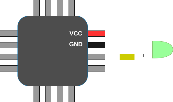
A microcontroller (uC or MCU) is a small computer that typically includes a CPU, RAM, Flash for storing firmware code, and some pins. Some of these pins power the MCU, typically marked as VCC and GND. Other pins communicate with the MCU using high and low voltages, and one of the simplest communication methods is to connect an LED to a pin: one end of the LED is grounded, the other end is connected in series with a current-limiting resistor, and then connected to the MCU signal pin. Setting the pin voltage high or low in the firmware code can make the LED blink:
Memory and Registers
The MCU’s 32-bit address space is divided into regions. For example, some memory regions are mapped to specific addresses, such as the MCU’s internal flash where firmware code instructions are read and executed. Other regions are RAM, also mapped to specific addresses, where we can read or write any values.
From section 2.3.1 of the STM32F429 datasheet, we learn that the RAM region starts at address 0x20000000 and has a total of 192KB. From section 2.4, we see that flash is mapped to 0x08000000, totaling 2MB, so the positions of flash and RAM are as follows:

The datasheet also shows many other memory regions, with their addresses given in section 2.3, “Memory Map”; for example, the “GPIOA” region starts at address 0x40020000 and has a length of 1KB.
These memory regions are associated with different peripheral circuits inside the MCU chip, controlling the behavior of peripheral pins in special ways. A peripheral memory region is a collection of 32-bit registers, each with 4 bytes of space, at specific addresses controlling specific functions of the peripherals. By writing values to the registers or writing a 32-bit value to specific addresses, we can control the behavior of the peripherals. By reading the values of the registers, we can obtain data or configuration from the peripherals.
The MCU usually has many different peripherals, with GPIO (General Purpose Input Output) being one of the simpler ones. It allows users to set MCU pins to output mode and then set them “high” or “low”; or to set them to input mode and read the pin voltage as “high” or “low”. There are also UART peripherals that can send and receive data using a serial protocol through two pins. There are many other peripherals as well.
In the MCU, the same peripheral typically has multiple “instances”, such as GPIOA, GPIOB, etc., which control different sets of MCU pins. Similarly, there are UART1, UART2, etc., allowing for multiple channels. On the Nucleo-F429, there are multiple GPIO and UART peripherals.
For example, the starting address of the GPIOA peripheral is 0x40020000. We can find the description of the GPIO registers in section 8.4 of the datasheet, which states that the GPIOA_MODER register offset is 0, meaning its address is 0x40020000 + 0. The register address format is as follows:
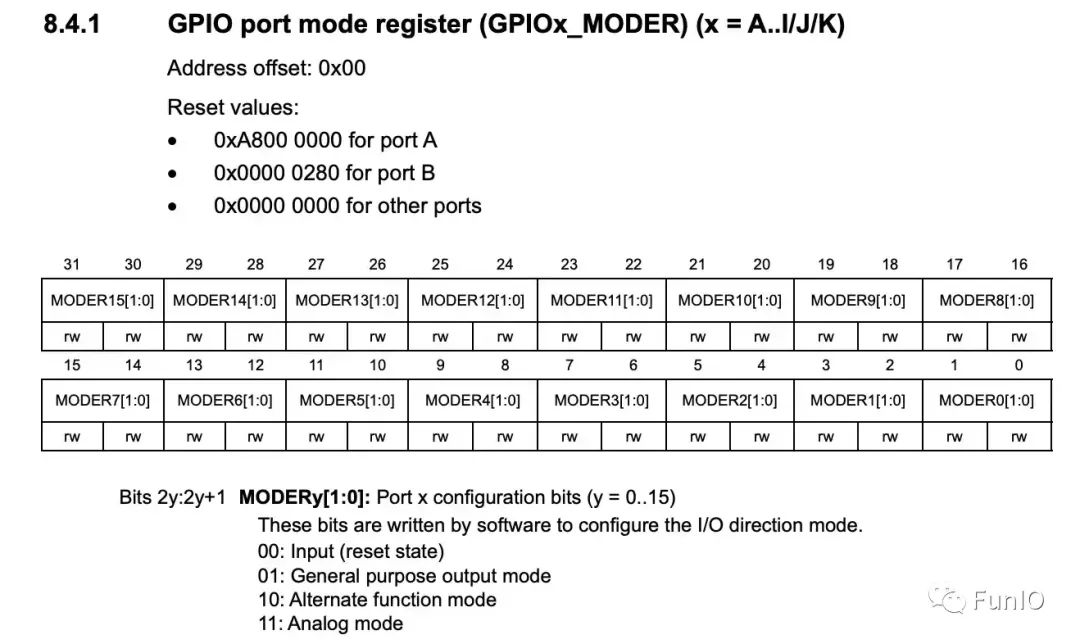
The datasheet shows that the MODER 32-bit register consists of 16 two-bit values. Therefore, a MODER register controls 16 physical pins, with bits 0-1 controlling pin 0, bits 2-3 controlling pin 1, and so on. This two-bit value encodes the pin mode: ’00’ represents input, ’01’ represents output, ’10’ represents alternate function—described elsewhere, and ’11’ represents analog pins. Since this peripheral is named ‘GPIOA’, the corresponding pin names are ‘A0’, ‘A1’, etc. For the peripheral ‘GPIOB’, the pins are named ‘B0’, ‘B1’, etc.
If we write a 32-bit value ‘0’ to the MODER register, it will set pins A0 to A15 to input mode:
* (volatile uint32_t *) (0x40020000 + 0) = 0; // Set A0-A15 to input mode
By setting individual bits, we can set specific pins to the desired mode. For example, the code below sets A3 to output mode:
  * (volatile uint32_t *) (0x40020000 + 0) &= ~(3 << 6);  // Clear bit range 6-7
  * (volatile uint32_t *) (0x40020000 + 0) |= 1 << 6;     // Set bit range 6-7 to 1
Let me explain the bit manipulation above. Our goal is to set the bits controlling pin 3 of the GPIOA peripheral, which are bits 6-7, to a specific value, which is 1 here. This requires two steps: first, we must clear the current value of bits 6-7, that is, set them to ‘0’, because these two bits may already have values; then, we set bits 6-7 to the desired value.
So, in the first step, we first clear bits 6-7 to ‘0’. How do we do this? In four steps:
- Make a number with N consecutive ‘1’s
- 1 bit is 1:
0b1 - 2 bits are 3:
0b11 - 3 bits are 7:
0b111 - 4 bits are 15:
0b1111 - And so on, for N bits, the value should be
2^N - 1. For 2 bits, the value is3, or written in binary as0b00000000000000000000000000000011 - Left shift the number. If we need to set bits X-Y, we left shift the number by X bits. In our case, left shift by 6 bits:
(3 << 6), resulting in0b00000000000000000000000011000000 - Invert: 0 becomes 1, 1 becomes 0:
~(3 << 6), resulting in0xb11111111111111111111111100111111 - Now, perform a logical