Source: Semiconductor Industry Observation
If we use Tape Out as the node for chip verification, it can be divided into Pre-Tape Out verification and Post-Tape Out verification.
Pre-Tape Out verification, known as Pre-Silicon verification, refers to verifying the functionality, performance, and power consumption of the chip based on various simulation platforms (FPGA, PXP, HAPS, ZeBU, etc.) and Bit Files to prepare for Tape Out.
Post-Tape Out verification, known as Post-Silicon verification, refers to the Foundry having completed the production of engineering samples. The engineering team receives the engineering samples and verifies them to determine whether the samples meet the design objectives, preparing for mass production of the chip.
During Tape Out, it is necessary to plan the engineering Wafer release strategy.
Taking TSMC as an example, typically, based on factors such as the scale of the SoC and Die Size, the company negotiates with TSMC on the number of engineering Wafers for each Tape Out, for example, 25 engineering Wafers, and the cost of these engineering Wafers is included in the Tape Out cost. Considering that most chips cannot achieve mass production directly from one Tape Out, it is necessary to plan the usage of these 25 engineering Wafers, taking into account at least the following requirements:
(1) Sufficient engineering chips for testing and verification;
(2) Reserve engineering Wafers for Metal Fix;
(3) Shorten chip verification time;
(4) Engineering failures;
(5) Specific project requirements. For example, under the premise of meeting the above requirements, reserve as many engineering Wafers as possible for mass production.
Taking a 12nm FFC SoC as an example, suppose this SoC involves 50 modules, with a chip Die Size of 30mm^2, using a 12-inch Wafer, with an MFU of 95%, it can be calculated that one Wafer can produce 2K chips. Assuming a yield of 85%, meaning CP and FT filter out 15%, the proposed engineering Wafer strategy is shown in Figure 1.
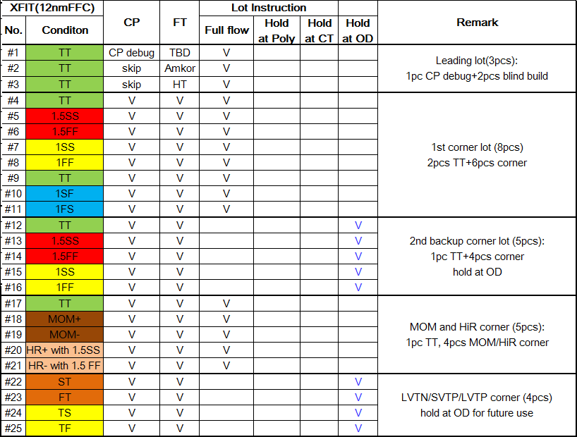
Figure 1 Engineering Wafer Strategy for a Certain Chip
Before explaining this table, let’s familiarize ourselves with some concepts.
The chip structure is like a building, at least including material selection (Corner) and base layer (Base Layer). The chip Corner selection is like choosing different materials to build a building. Chip manufacturing is a physical process that involves process deviations. Depending on the process settings and the switching speeds of PMOS and NMOS, it is categorized into different Corners, with typical terms like TT, FF, SS, while different levels of FF and SS are set based on the magnitude of deviations, such as 2FF indicating a shift of 2 Sigma towards faster, and 3SS indicating a shift of 3 Sigma towards slower (as to why different Corners are made for chips, that will be discussed in another topic).
Selecting Corners can be understood as selecting different materials to build a building; once the decision is made, it cannot be changed, as referenced in Table 1:
(1) Hold OD, which can be understood as having selected the location for a tall building, where the material can still be changed as needed, but the process can also be changed;
(2) Hold at Poly, meaning the location and material have been selected, but the foundation has not yet started, i.e., the chip’s Base Layer has not yet begun;
(3) Hold at Count, meaning the foundation has been laid and cannot be changed, but the connections between floors can be modified, i.e., Metal layer modifications can be made.
Now, let’s look back at Table 1.
The first batch #1~#3, Leading Lot, 3PCS TT, Full flow run to end. Wafers #1~#3 do not perform CP and FT testing, running directly to the end. One of the Wafers is used for PC debugging, sent to the packaging factory to produce Bump, and this Wafer does not need to be cut, used for debugging the PC program. The other two Wafers, after producing Bump, are cut and packaged, and the first batch of chips does not perform FT testing, they are blindly packaged and sent back (Why are Leading Lots using TT and not doing CP? Why can’t all Leading Lots do FT testing?).
The second batch #4~#11, First Corner Lot, performs CP and FT testing, Full flow run to end. Because it includes Corner Wafers, different machines are used compared to the first batch. #4 and #9’s TT are used to verify differences between different machines under the same Corner. The remaining six Wafers are Corner Wafers.
The third batch #12~#16 is a Backup Lot, including various Corners and Hold at OD. The 12nm process is not yet mature, to prevent engineering issues from the first two batches of Wafers, backup is made, and preparations for Metal Fix are also made. Choosing Hold at OD rather than keeping the original Wafers is to ensure that the process can be changed according to needs, and considering that once engineering issues arise, or Metal Fix is needed, starting from OD reduces the time for chips to come back (Why not Hold at Poly?).
The fourth batch #17~#21 is used to verify MON+/- and HR+/- processes, Run to end, performing CP and FT testing.
The fifth batch #22~#25 Hold at OD as backup. Considering that the return time for engineering samples is longer than that for mass production chips, if there is customer demand and the previous samples have met chip verification requirements, these four Wafers can be shipped as mass production Wafers.
In summary, the usage of these 25 engineering Wafers in this case considered various scenarios such as practicality and timeliness, but it is not without flaws; it is merely a decision weighed against various possibilities based on the specific situation of this Tape Out.

Public Account ID: imecas_wx