This is the 145th content shared by the platform.

The background of the development of Analog-to-Digital Converters (ADC) mainly stems from the rapid advancement of digital technology.
In the early days, electronic systems were mostly based on analog signal processing. However, with the rise of computer technology and digital signal processing theory, there was a need to convert analog signals from the real world, such as sound, temperature, pressure, and other physical quantities, into digital signals for efficient processing by digital systems. For example, in the field of communications, to achieve long-distance transmission and accurate regeneration of signals, it is necessary to digitize analog voice signals. In industrial control, the analog data obtained by sensors also needs to be converted into digital form for automated control and precise monitoring by computer systems. Thus, the Analog-to-Digital Converter was born to bridge this critical gap between the analog and digital worlds.


1. Overview of Analog-to-Digital Converters


An Analog-to-Digital Converter (ADC) is a device that converts continuous-time, continuous-amplitude (analog) signals into discrete-time, discrete-amplitude signals (digital signals), commonly referred to as A/D converters or ADCs.
The working principle of an ADC mainly includes the following steps:
Sampling: This is the first step in the analog-to-digital conversion process. The sample-and-hold circuit discretizes the input continuous analog signal at specific time intervals to obtain the amplitude of the analog signal, resulting in a series of sampled values. The sampling frequency must satisfy the Nyquist theorem, which states that the sampling frequency must be at least twice the highest frequency of the signal to avoid aliasing and ensure accurate reconstruction of the analog signal. For example, for an analog signal with a maximum frequency of 1 kHz, the sampling frequency should be at least 2 kHz.
Quantization: This step converts the sampled continuous analog signal amplitudes into discrete digital signals. The quantization process involves dividing the range of the analog signal amplitudes into several discrete levels, each corresponding to a specific digital value. The precision of quantization is determined by the resolution of the ADC, typically expressed in bits (bit). For example, an 8-bit ADC can represent 256 different values (2^8). There are methods of quantization such as linear quantization and nonlinear quantization; linear quantization divides the sampled values at equal intervals, while nonlinear quantization adapts to the characteristics of the signal, such as using logarithmic quantization for audio signals to better match human hearing perception.
Encoding: This step converts the quantized digital signal into binary code for subsequent digital processing and storage. Common encoding methods include binary encoding and Gray code, implemented by an encoder that maps each quantization level to the corresponding binary code.
Output: Finally, the encoded binary digital signal is output to digital circuits or microprocessors for further processing, analysis, storage, or transmission.
Based on the working principle of ADCs, they can be classified into direct ADCs and indirect ADCs. Direct ADCs convert analog signals directly into digital signals, such as parallel comparator ADCs and successive approximation ADCs. Indirect ADCs convert analog signals into an intermediate variable, such as time or frequency, and then convert that intermediate variable into a digital quantity, such as dual (slope) integration ADCs.
The block diagram of an ADC system is shown below.
Figure 1: The ADC consists of a sampler and quantizer.


2. The Analog-to-Digital Converter in STM32F407


STM32F407 is a high-performance 32-bit MCU based on the ARM core, featuring three 12-bit successive approximation ADCs (SAR ADC) with a maximum sampling rate of 2.4MSPs. The successive approximation ADC is a medium sampling frequency (1~50MSPs) and medium resolution (10~18 bits) ADC structure. Due to its simple structure and low power consumption, it is widely used in sensor detection and industrial control.
This ADC has up to 19 multiplexed channels, capable of measuring signals from 16 external sources, 2 internal sources, and the VBAT channel. The A/D conversion of these channels can be performed in single, continuous, scan, or discontinuous sampling modes.
The following diagram shows the block diagram of a single ADC.
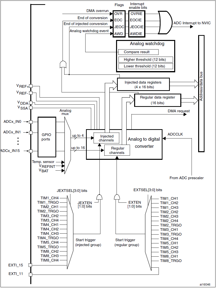
Figure 2: Block diagram of a single ADC.
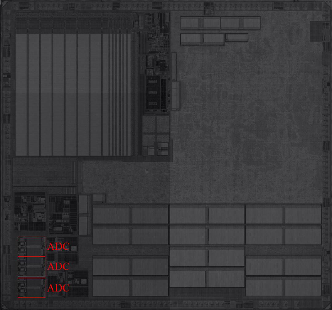
Figure 3: Overview of STM32F407 (DF).
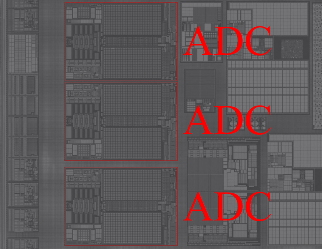
Figure 4: Partial overview of STM32F407 (POLY).
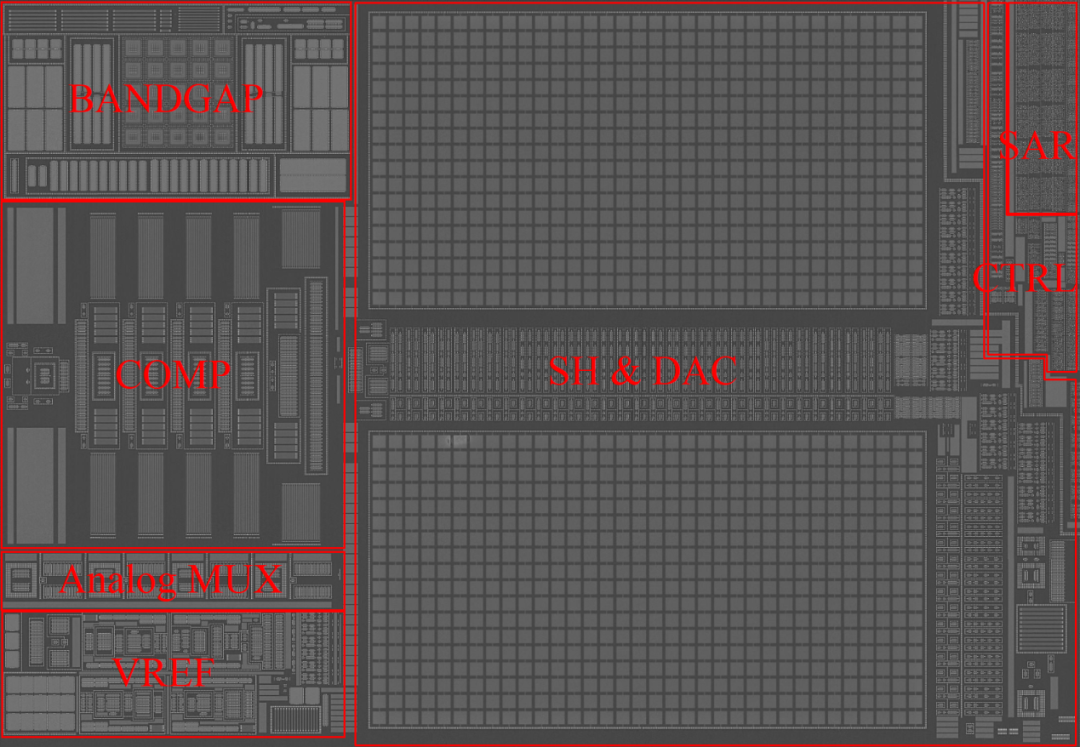
Figure 5: Functional modules of the SAR ADC in STM32F407.
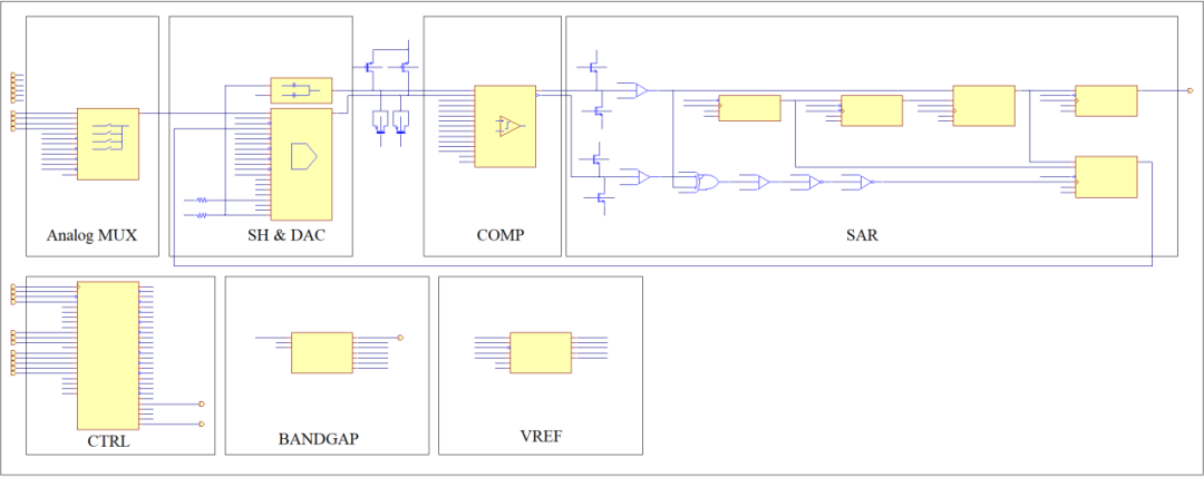
Figure 6: Circuit diagram of the SAR ADC in STM32F407.
3. Simulation Analysis of the SAR ADC in STM32F407
3.1 Simulation of System Structure and Working Principle
The ADC in STM32F407 is an improved successive approximation ADC that employs a charge redistribution structure, utilizing a binary search algorithm. Its main advantage is the integration of the sampling circuit and the hold circuit, significantly reducing design complexity. Additionally, its input signal amplitude is larger than that of other structures of SAR ADCs, capable of reaching an input swing from 0 to VDD.
The structure of the charge redistribution SAR ADC is shown in Figure 7, consisting of a binary-weighted capacitor network (with capacitance values in a geometric series, increasing in binary multiples), a series of analog switches, a comparator, and digital control logic. To complete a signal conversion, it requires both sampling and holding modes, determining the final digital output through binary search.

Figure 7: System structure diagram of the SAR ADC.
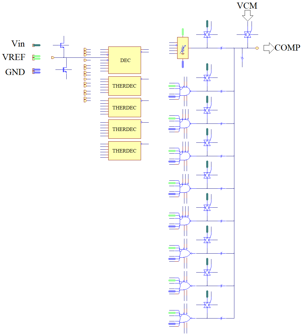
Figure 8: Part of the binary-weighted capacitor network used in the ADC of STM32F407.
1. Sampling Mode
As shown in Figure 7, in sampling mode, the upper plate of the capacitor network is connected to the common mode level VCM, and the lower plate is connected to the analog input signal Vin, thus the upper plate will store a certain amount of charge Qup, proportional to Vin:
Qup = (VCM – Vin) × Ctot;
Where Ctot is the total capacitance value of the binary-weighted capacitor network.
2. Hold Mode
In hold mode, the upper plate of the capacitor network is disconnected from VCM, and the upper plate will not connect to any voltage source before re-sampling, thus the accumulated charge on the upper plate will remain unchanged during subsequent operations, meaning the voltage difference between the upper and lower plates will remain constant. Then, starting from the highest bit, the values of each bit are determined sequentially using binary search until the lowest bit result is obtained. Determining each bit value requires two operations: charge redistribution and comparison. For the highest bit, the process of these two operations is described in conjunction with simulation results. The voltage Vin to be converted is set to 1.8V, and the ADC range (Vref) is set to 0~3.3V.
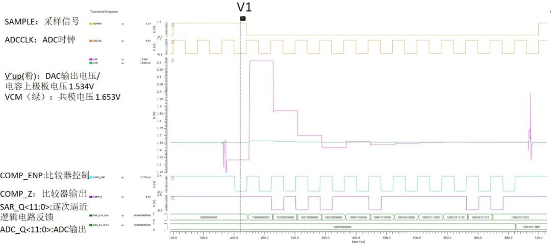
Figure 9: Analog-to-Digital conversion process (at time V1).
① Charge Redistribution
When determining the highest bit value, the highest bit is set to 1, and the other bits to 0. For the value of SAR_Q<11:0> at time V1, it is 100000000000. In the corresponding circuit, the highest bit switch SN is connected to Vref, while all other lower plate switches are connected to GND. The previous sampling phase has obtained a fixed voltage difference between the upper and lower plates:
ΔU=Qup× Ctot = V’up- V’down;
ΔU= VCM – Vin= V’up- V’down;
Since the capacitance value corresponding to SAR_Q<11> occupies 1/2 of the total capacitance value of the binary-weighted capacitor network, the voltage of Vref/2 is added to the lower plate of the capacitor network:
V’down= Vref/2;
Thus, the charge on the upper plate of the capacitor network will redistribute, resulting in a new upper plate voltage value:
V’up = VCM – Vin + Vref/2
Calculating gives V’up = 1.5V, and this voltage is measured as 1.534V in the circuit at time V1.
② Comparison
After charge redistribution, the obtained voltage value is compared with VCM: if V’up<VCM:
Then VCM – Vin + Vref/2<VCM;
Simplifying gives Vin>Vref/2, thus the highest bit is 1;
If V’up>VCM:
Then VCM – Vin + Vref/2>VCM;
Simplifying gives Vin<Vref/2, thus the highest bit is 0;
If the highest bit is 1, the corresponding switch SN remains unchanged; if the highest bit is 0, then SN connects to GND.
In the circuit, at time V1, after charge redistribution, at the first rising edge of COMP_ENP, V’up is compared with VCM. At this point, V’up<VCM, so the comparator outputs 1, indicating that the highest bit value is 1.
Then the comparison for the next bit is performed.
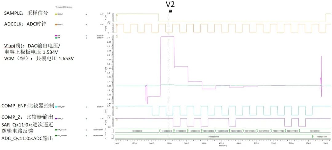
Figure 10: Analog-to-Digital conversion process (at time V2).
First, set the second highest bit to 1, and the remaining bits to 0, which means the corresponding switch SN-1 switches from GND to Vref, while others remain unchanged. At this point, the charge on the upper plate of the capacitor network will redistribute, resulting in a new voltage value:
V’up = VCM – Vin + Vref * (2N-1 * MSB + 2N-2)/2N = 2.325V
This voltage is measured as 2.212V in the circuit at time V2. Then, at the rising edge of COMP_ENP, a comparison is made, and since V’up>VCM, the value of the second highest bit is 0.
Continuing this process, all bit values can be determined. Since the ADC has a precision of 12 bits, a total of 12 comparisons are needed to obtain the final ADC output. From the above diagram, it can be seen that when Vin=1.8V, the converted digital code is 100010111001.
The above describes the conversion process of the ADC with a fixed input voltage. If we gradually increase the input Vin, we obtain the following results:
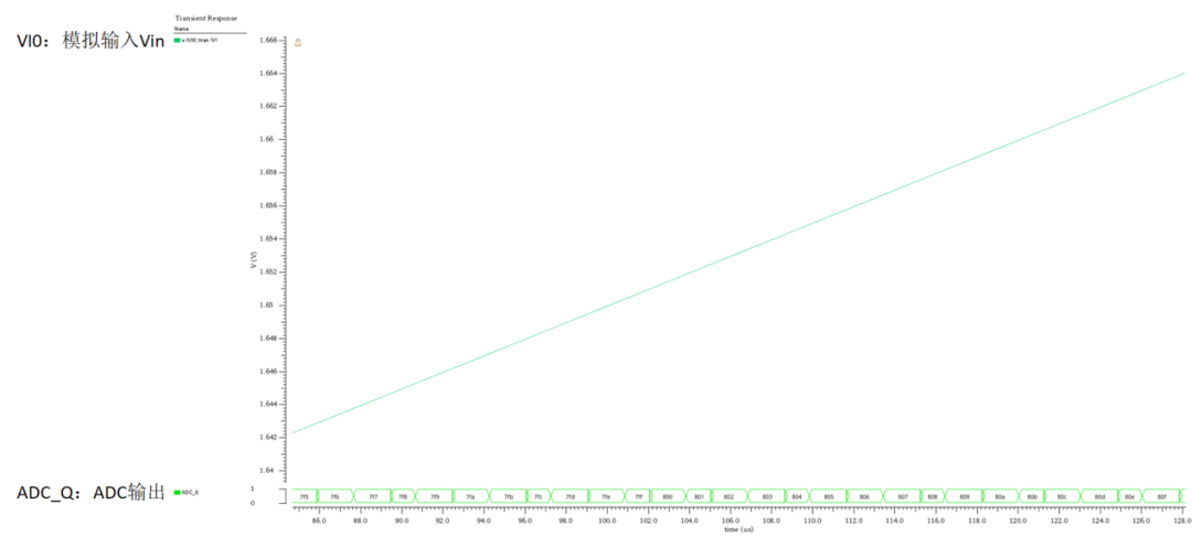
Figure 11: ADC Input and Output (12bit).
As the Vin input gradually changes, the values converted to digital signals by the ADC also change gradually. As long as the frequency of the input Vin and the sampling frequency satisfy the Nyquist sampling theorem, a digital signal without missing codes can be obtained.
3.2 Simulation of 6-bit Resolution
One of the features of the SAR ADC in STM32F407 is that it can be configured for 12-bit, 10-bit, 8-bit, or 6-bit resolution. With reduced resolution, the quantization time per conversion also decreases from the original 12 ADCCLK cycles to 6 to 10 ADCCLK cycles, allowing for faster conversions.
The following diagram shows the ADC resolution selection control circuit. By modifying the resolution selection port, the clock signal in the ADC circuit can be changed to achieve the desired resolution configuration.
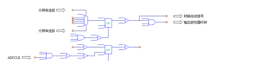
Figure 12: ADC Resolution Selection Control Circuit.
Based on the 12-bit simulation circuit, modifying the control to configure the resolution to 6 bits while keeping other inputs unchanged, the following results were obtained:
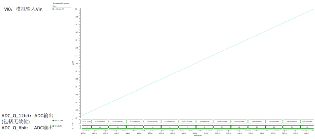
Figure 13: ADC Input and Output (6-bit Resolution).
After loading all outputs from the ADC, it can be seen that the lower 6 bits of the output bus are constantly 0, indicating invalid bits. Removing the invalid bits yields the 6-bit bus as the current ADC output result.
4. Conclusion
The above is a simulation analysis of the SAR ADC conversion process in the STM32F407. Among the various possible applications of ADCs, the above example, although a small one, is quite representative.
With its unique analog-to-digital conversion capabilities, ADCs are widely used in sensor data acquisition, signal processing, and control systems.

Previous Exciting Recommendations
In-Depth Analysis | Understanding the Working Principle of Chip Clock Locking PLL Phase-Locked Loop in One Article
2024-10-15

Shocking! This small module can manipulate the heartbeat of the chip, revealing the ultimate secret of the OSC oscillator!!
2024-12-04