1. Heterogeneous Computing Units: The Collaborative Logic of the Car’s “Brain”
1. What is Heterogeneous Computing?
The “heterogeneous computing” in automotive SoC chips refers to the integration of multiple processing units (such as CPU, GPU, AI accelerators, etc.) within the same chip, collaborating to meet the diverse needs of vehicles—from real-time control (like braking) to complex AI inference (like autonomous driving). Analogous to the human nervous system, the CPU serves as the logical decision-making center, the GPU specializes in visual processing, and the AI accelerator acts as a rapid-response intuitive system.
Typically, an automotive SoC chip includes the following major modules: processors, memory, and peripheral I/O, etc. 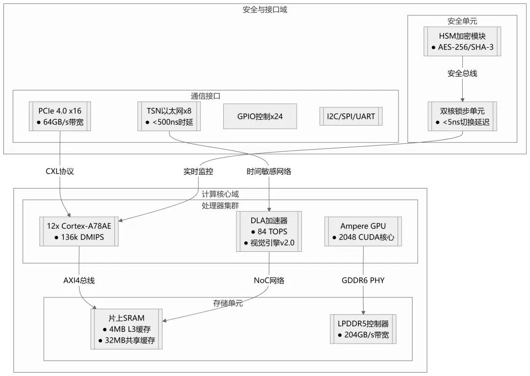
2. Core Components and Functions of Processors
-
CPU (Central Processing Unit)
-
Definition: Responsible for system-level task scheduling (such as sensor data fusion) and general logic operations (such as path planning).
-
Evaluation Metrics:
DMIPS (Million Instructions Per Second): Measures the ability to process instructions per second, for example, the CPU cluster of NVIDIA Orin-N can reach 136k DMIPS;
Real-time Performance: The response delay for critical tasks must be less than 10 microseconds (such as in automatic emergency braking systems).
-
GPU (Graphics Processing Unit)
-
Definition: Specializes in graphics rendering (dashboard display) and parallel computing (BEV bird’s-eye view generation).
-
Evaluation Metrics:
-
FLOPS (Floating Point Operations Per Second): Measures graphics processing capability
-
Pixel Fill Rate: Determines the detail level of images.
-
AI Accelerator (NPU/BPU)
-
Definition: A dedicated processor optimized for neural networks, used for efficiently executing deep learning algorithms (such as lane line recognition).
-
Evaluation Metrics:
-
TOPS (Trillions of Operations Per Second): Theoretical peak computing power, for example, Horizon Journey 6P reaches 560 TOPS;
-
Energy Efficiency Ratio (TOPS/W): Computing power per unit of power consumption, Journey 6P achieves an energy efficiency ratio of 6.8 TOPS/W, far exceeding traditional GPUs.
-
Application Scenarios: Huawei Ascend NPU supports real-time decision-making for urban no-map navigation (NOA).
2. Storage and Interface Design: The Data Highway’s System Engineering
1. Storage Architecture Design
The storage system of automotive SoCs must meet real-time, reliability, and capacity requirements simultaneously, with core units including:
-
SRAM (Static Random Access Memory):
Definition: Volatile storage based on flip-flop structures, with extremely fast read/write speeds (<10ns latency).
Function: Used for CPU cache (L1/L2/L3) and as a temporary data pool for AI accelerators.
-
DRAM (Dynamic Random Access Memory):
Definition: Volatile storage that stores charge through capacitors and requires periodic refreshing.
Function: Main memory (e.g., LPDDR5 with a bandwidth of 204GB/s), supporting real-time loading of AI models, NVIDIA Orin X uses a 2048-bit bus design.
-
NOR Flash:
Definition: Non-volatile storage that supports XIP (Execute In Place) technology, with an erase/write life of about 100,000 cycles.
Function: Stores boot code (Bootloader), firmware, and critical configuration parameters, Tesla HW4.0 uses it to store the FSD chip initialization program.
-
NAND Flash:
Definition: High-density non-volatile storage, available in SLC/MLC/TLC types (erase/write life of 10,000 – 100,000 cycles).
Function: Large-capacity data storage (e.g., high-precision maps).
-
eMMC (Embedded MultiMediaCard): A non-volatile storage solution designed specifically for embedded systems, standardized by JEDEC (Joint Electron Device Engineering Council). Its core feature is the integration of NAND flash, a controller, and a standardized interface into a single BGA package, simplifying the storage design of embedded devices.
Function: A low-cost storage solution commonly used in in-vehicle infotainment systems (IVI), such as storing user data for BYD DiLink systems.
2. Sensor Interface Solutions
-
MIPI-CSI-2: Concept: A camera serial interface standard established by the Mobile Industry Processor Interface Alliance, using differential signaling to reduce interference. Function: Supports up to 8K resolution input (4-lane configuration), Tesla HW4.0 connects 8 cameras through this interface.
-
GMSL III: Concept: Gigabit Multimedia Serial Link, supports long-distance transmission (30 meters @ 3Gbps), using coaxial cables to resist interference. Function: Transmits LiDAR point cloud data, such as NIO Aquila’s super-sensing system connecting to Innovusion LiDAR.
-
LVDS (Low-Voltage Differential Signaling): Concept: A low-power, interference-resistant differential signaling interface with a bandwidth of up to 1Gbps. Function: Raw data return from millimeter-wave radar, Bosch’s fifth-generation radar uses this protocol.
3. Communication Interface Solutions
-
PCIe 4.0: Concept: A high-speed bus for peripheral component interconnect, supporting a transmission rate of 16GT/s, using a point-to-point topology. Function: High-speed interconnection between domain controllers (such as between the intelligent driving domain and the cockpit domain), Horizon Journey 6 supports PCIe 4.0×4 channels.
-
TSN Ethernet: Concept: Time-Sensitive Networking protocol, supports time synchronization, with latency <1ms. Function: Real-time control command transmission (such as line control braking), Huawei MDC platform uses TSN to connect actuators.
-
I2C/SPI: Concept: I2C is a two-wire bus (SCL/SDA), SPI is a four-wire full-duplex bus (MOSI/MISO/SCK/CS). Function: Connects low-speed devices such as temperature sensors and IMUs, for example, Tesla’s battery management system monitors cell status via I2C.
-
UART/GPIO: Concept: UART is an asynchronous serial interface, GPIO is a general-purpose input/output pin. Function: Debugging interface (such as log output), hardware status monitoring (such as fan speed control).
3. Safety Modules: The Underlying Foundation of Automotive-grade Design
1. Functional Safety Mechanisms
-
Hardware Security Module (HSM): An independent encryption unit that supports national cryptographic algorithms (such as SM2/3/4), with keys stored in a physically isolated area (Tesla HW4.0 uses a dedicated security island).
-
Dual-Core Lockstep Design: Two sets of computing cores compare results in real-time, switching immediately upon detecting anomalies (Infineon TC397 MCU ensures ASIL-D level safety).
2. Certification System
-
AEC-Q100: Reliability testing standard covering extreme environmental simulations such as high temperature and vibration;
-
ISO 26262: Functional safety process certification, spanning from chip design to mass production (Horizon Journey 6 series has passed ASIL-D certification).
4. Automotive Companies’ Self-Developed SoC Practices and Benchmark Cases
1. Tesla FSD HW4.0
-
Heterogeneous Computing: 5nm process integrates 3 NPUs, with computing power exceeding 700 TOPS, focusing on pure vision solutions (Occupancy Network modeling);
-
Storage Interface: Supports 5 million pixel camera input, detection distance increased to 424 meters;
-
Safety Design: Independent security island + shadow mode redundancy, fault switching time <1ms.
-
Advantages: Vertically integrates autonomous driving algorithms and hardware, Dojo supercomputer accelerates data closed-loop iteration.
2. Huawei MDC Platform
-
Heterogeneous Computing: Ascend NPU (400 TOPS) and MCU hard-linked, with deterministic latency <10μs;
-
Interface Expansion: Compatible with 14 cameras + TSN Ethernet, liquid cooling supports 120W power consumption;
-
Safety Architecture: HSM integrates national cryptographic algorithms, with key tiered management.
-
Advantages: Full-stack self-development achieves deep adaptation of software and hardware, supporting customized needs of automotive companies.
3. Horizon Journey 6 Series
-
Heterogeneous Computing: BPU Nash architecture optimizes sparse computing, leading the industry in computing power density;
-
Storage Design: Triple cache + LPDDR5, data transfer efficiency improved by 30%;
-
Safety Strategy: Virtualization isolates non-secure tasks, certified by ASIL-D.
-
Advantages: Aiming at the 150,000-300,000 yuan vehicle market, planning to ship over 10 million units by 2025.
5. Industry Chain Panorama Analysis
1. Upstream: Core Technology Barriers
-
IP Cores: ARM architecture occupies the mainstream (90% share), domestic RISC-V (SinoChip Technology) accounts for less than 10%;
-
EDA Tools: Synopsys and Cadence monopolize 73% of the domestic market, Huada Empyrean breaks through the verification stage.
2. Midstream: Manufacturing and Design Game
-
Wafer Foundry: TSMC’s 5nm supports Tesla HW4.0 mass production, SMIC’s 14nm accelerates automotive verification;
-
Design Models: Tesla adopts IDM (Integrated Device Manufacturing), Horizon chooses Fabless (focusing on design).
3. Downstream: Competition and Cooperation between Automotive Companies and Tier 1 Suppliers
-
Cooperation Models: Black Sesame Intelligence + Intel launched a cabin-driving integration solution, Qualcomm + Zhongke Chuangda developed a complete vehicle OS;
-
Domestic Substitution: By 2025, the market share of domestic SoCs is expected to increase from 5% to 35% (Horizon and Huawei leading).
6. Future Trends and Challenges
1. Directions for Technological Breakthroughs
-
Chiplet Heterogeneous Integration: Intel’s SDV SoC increases computing power density by 3 times through chip stacking;
-
Software-Defined Chips: Horizon opens BPU IP licensing, supporting dynamic loading of algorithms.
2. Evolution of Market Landscape
-
High-End Market: Tesla and NVIDIA (Thor chip) compete for the 2000 TOPS computing power track;
-
Mid-Range Market: Horizon, NVIDIA (ORIN-N), and TI (TDA4 series) seize the integrated control domain with cost-effectiveness.