
Click the top to follow us!
01
Introduction
Common NFC tags generally do not require power; they only need to be brought close to a mobile phone with NFC functionality. The coil antenna on the phone induces mutual inductance with the coil antenna on the tag, causing a changing current of 13.56M to flow through the phone’s coil. This generates an induced electromotive force on the tag, acting like a power source, allowing the chip on the tag to start working. The phone can then read and write data to it, and after power is cut off, the written data will be retained. The tag I designed requires power and also features an I2C interface.
02
Application Description
What can a tag with an I2C interface do? How can it be applied? With the I2C interface, it can be connected to a microcontroller. This way, the microcontroller can write data to the tag via I2C, which can then be read by the mobile phone’s NFC function. Alternatively, the mobile phone can write data to the tag using standard NFC functionality, and the tag can then relay this data to the microcontroller via I2C. Ordinary tags can only store information that does not change by itself; the next time the phone reads it, it will still show the same information. However, when combined with a microcontroller, a tag with I2C can process real-time information and pass it to the tag, so the information read by the phone can be different each time. For example, a microcontroller can collect temperature data or perform certain counts, which can then be read by the phone to gather information.
03
Schematic and PCB Design
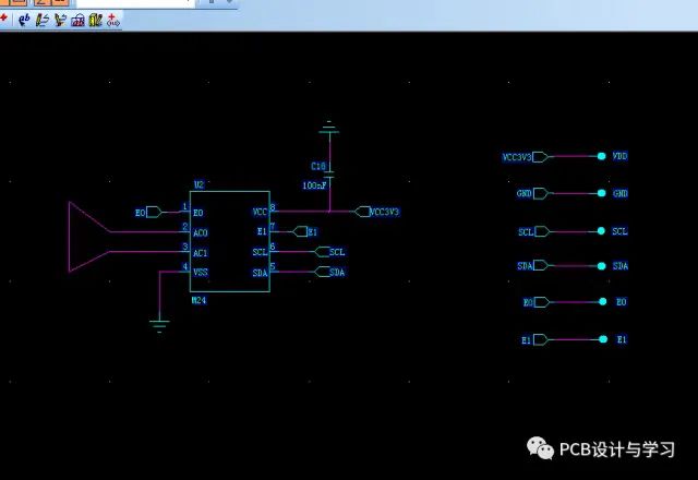
Schematic
PCB
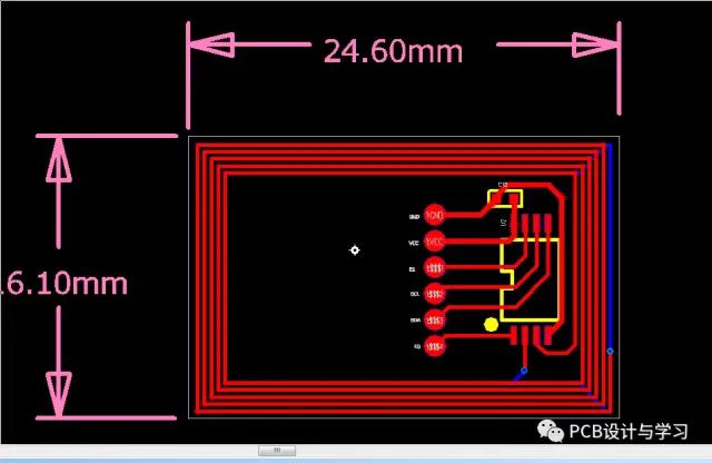
Above are the schematic and PCB design of the NFC tag with I2C. Interested friends can reply “NFC with I2C” on the official account homepage to get the download link or download it from the group.

Scan to follow me
Let’s appreciate the charm of science together

Tap to Share

Tap to Collect

Tap to Like

Tap to View