❝
Introduction: This article presents a solution to implement the main functions of the 555 timer based on the DAC53701. The DAC53701 has significant advantages in signal precision.
01 DAC Replacing 555
1. Question about 555 Circuit
Two days ago, I saw a student asking how to improve the precision of the square wave signal generated by the 555 timer circuit in the public account backend.
❝
Zhuo, how can the frequency of the square wave generated by the 555 timer be more precise?
Of course, if the student asking the question now understands the working principle of the 555 timer circuit and knows the relationship between the frequency of the square wave signal and the external resistor and capacitor components, they can find ways to improve the precision of the 555 timer circuit.
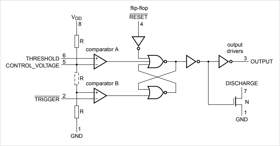
The factors affecting timer precision can be divided into two aspects.
-
System Error: This refers to the accuracy of the internal reference voltage source of the 555 timer circuit, the precision of timing resistors, and capacitors, which affect the frequency of the square wave. Generally, if high output current from the 555 is not required, choosing the CMOS version of the 7555 series timer circuit, operating at a voltage above 5V, can achieve a frequency better than 5%. -
Random Error: This includes environmental temperature affecting changes in external R and C components, circuit noise causing phase jitter in the output square wave, etc.
To ensure that the output frequency accurately reaches the desired frequency, it is often necessary to add a precision adjustable resistor to the peripheral resistor to adjust the hardware to achieve the required frequency accuracy.
In fact, if it weren’t for cost issues, using an 8-pin or even 6-pin microcontroller to generate the required frequency square wave might be more convenient.
2. Smart DAC
While browsing literature on improving the precision of the 555 timer online, I came across an engineering application report from TI: Considering TI Smart DACs As an Alternative to 555 Timers[5], which presents a method to realize the functions of the 555 using TI Smart DAC.
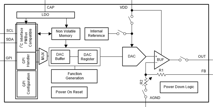
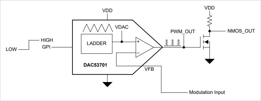
This 10-bit DAC, model DAC53701, is known as a Smart DAC, which integrates not only the high-precision reference power supply needed for DACs, but also the DAC conversion circuit, I2C, and SPI interface circuits. Compared to other DACs, it has the following features:
-
Internal power-down protection memory to save all setting parameters; -
Includes a waveform generator capable of producing triangle, sawtooth, and square wave signals; -
Output buffer amplifier with feedback pin brought out externally; -
Programmable input ports;
The chip is also in an 8-pin package. The internal functional reference diagram is shown below.
3. Implementing 555 Functions
Since the DAC53701 has an internal EEPROM memory, the functions set via I2C/SPI can automatically restore after power-up. Below are the circuit configurations to realize several main functions of the 555 timer.
1. Output Square Wave Signal
This part utilizes the waveform generator function of DAC53701. By setting it up, a triangle wave signal is generated internally. The corresponding frequency is calculated from the following formula:
Where:
-
: is given by the internal register (time per step); -
: is the value encoded by the DAC output; -
: is the change in DAC value per step;
All the above values are provided by the power-down hold register of the DAC53701.
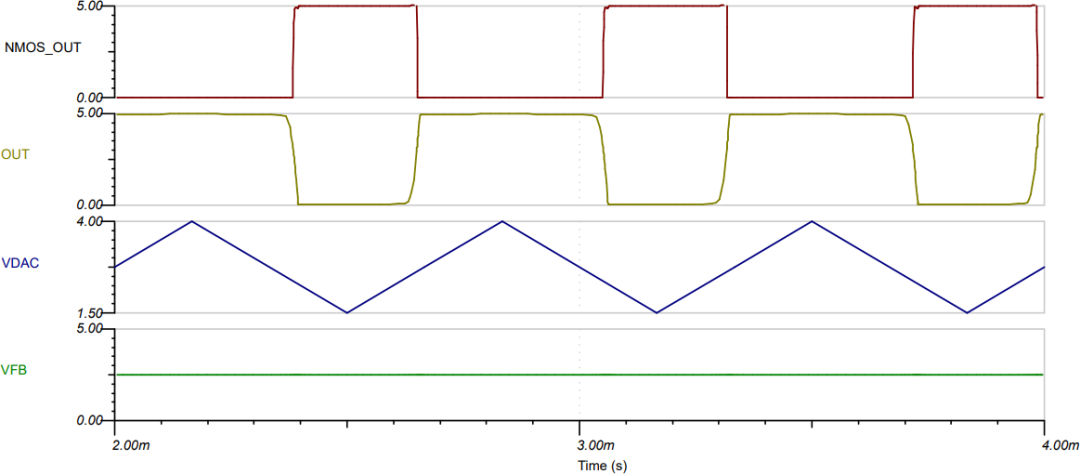
The circuit for generating output square wave using DAC53701 is shown in the figure below. The output buffer operational amplifier of DA53701 is switched to comparator mode, with an external voltage divider providing the reference voltage for the comparator. Thus, after the internal triangle wave is compared, a square wave will be generated at the output port. This is then amplified and cleaned up through an NMOS stage to achieve a better square wave shape.
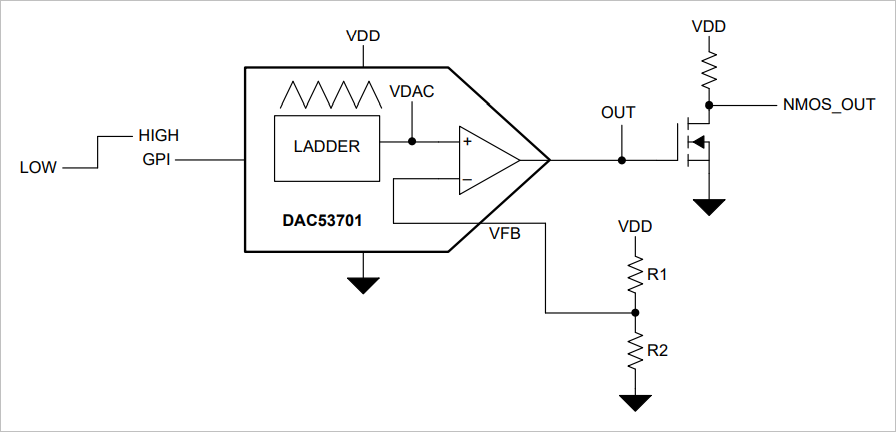
The following figure shows the square wave signal generated by DAC53701 at 1.5kHz with a duty cycle of 60%. Changing the voltage divider can alter the duty cycle of the output square wave, and changing the internal register value of the DAC can adjust the output frequency.
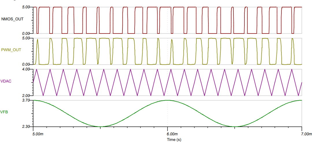
2. Output PWM Signal
Based on the above circuit, changing can generate a PWM waveform with a variable duty cycle. It can be seen that the duty cycle of the output PWM waveform is linearly related to the input voltage. In contrast, the PWM waveform produced by changing the CONT voltage in the 555 circuit does not have a strict linear relationship with the CONT voltage.
3. Schmitt Comparator
In the 555 circuit, connecting PIN6 (THRESHOLD) and PIN2 (/TRIGGER) together as input makes the output of the 555 a comparator with hysteresis characteristics (Schmitt Trigger), usually used to shape signal waveforms or convert the original analog signal into digital signals of high and low levels.
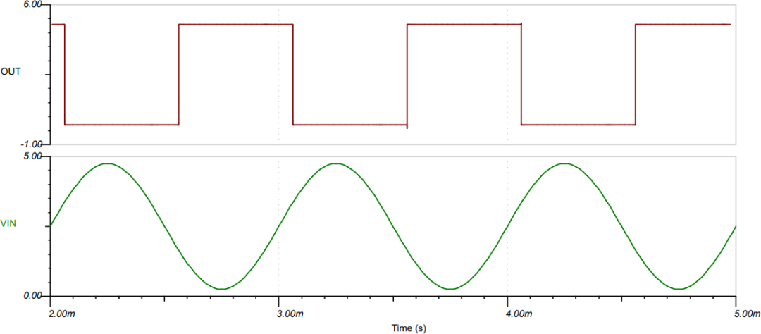
The following figure shows the working waveform of the 555 circuit converting an input sine wave into a square wave as a hysteresis comparator.
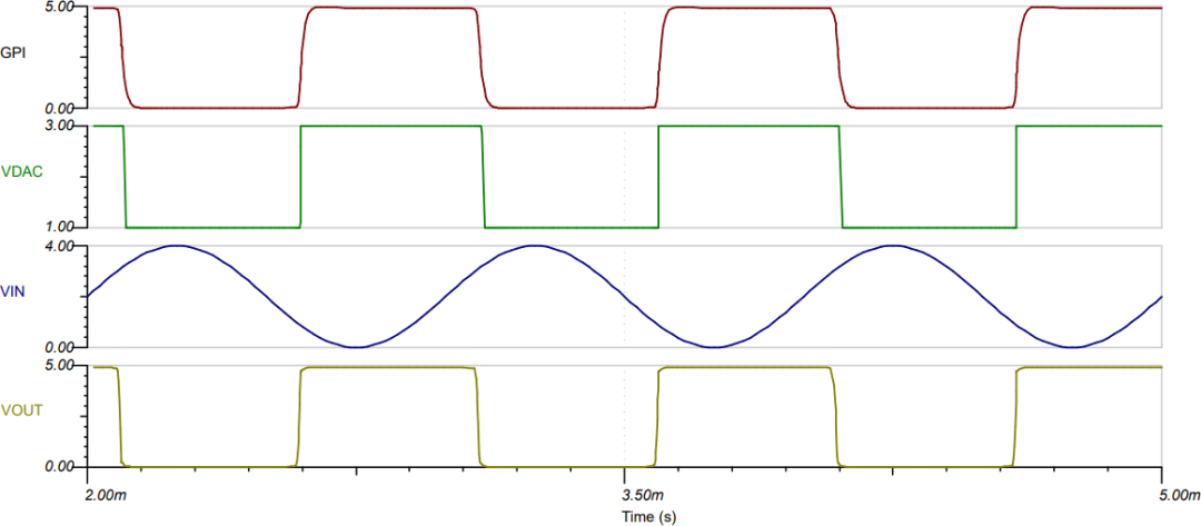
Using the GPI function of DAC53701, it can be configured as a Schmitt comparator with hysteresis characteristics. GPI can be used to select the output value of the internal DAC, thus changing the value of the internal comparator V+. By connecting VOUT back to GPI, the internal comparator’s reference voltage can be dynamically altered. By setting the appropriate DAC value corresponding to GPI, this feedback will create hysteresis characteristics. The RC filter in the feedback loop can eliminate jitter during the comparator switching process.
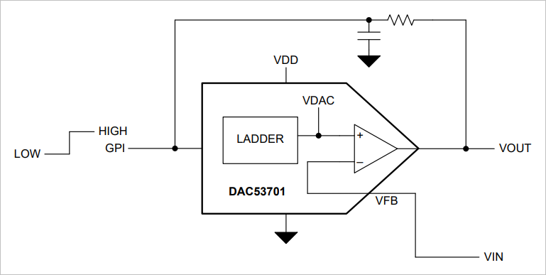
Since the output voltage of the internal DAC of DAC53701 can be set through internal registers, the two reference voltage values of the hysteresis comparator can be changed. In contrast, the hysteresis comparator voltages of the 555 timer can only be 1/3 and 2/3 of the operating supply voltage. This flexibility makes DAC43701 more adaptable.
The following figure shows the voltage signal waveforms at various points in the circuit when DAC53701 is used as a hysteresis comparator.
By utilizing hysteresis characteristics, along with R and C circuits, monostable, bistable, and astable circuits can also be formed.
4. Conclusion
Using the DAC53701 to achieve common functions of the 555 not only provides strong flexibility in parameter configuration, with main oscillation frequency and hysteresis voltage being internally programmable, but also does not rely on external resistor and capacitor components, thus achieving high precision. For example, at room temperature, the frequency precision exceeds 1%, which is better than common 555 timer circuits.
Of course, compared to traditional 555 circuits, the DAC53701 also has certain limitations, such as its relatively high price, narrow operating voltage range (1.8V – 5.5V), and slightly higher static power consumption than CMOS 555 integrated circuits.
※ Conclusion ※
This article presents a solution to implement the main functions of the 555 timer based on the DAC53701. The DAC53701 has significant advantages in signal precision.
References
**555 timer – large inaccuracies with precision components [duplicate: https://electronics.stackexchange.com/questions/530405/555-timer-large-inaccuracies-with-precision-components
[2]LTC6900CS5: https://pdf1.alldatasheet.com/datasheet-pdf/view/117573/LINER/LTC6900CS5.html
[3]USING THE 555 TIMER IC IN SPECIAL OR UNUSUAL CIRCUITS: https://www.nutsvolts.com/magazine/article/using-the-555-timer-ic-in-special-or-unusual-circuits
[4]555 Precision Timers Datasheet: https://www.ti.com/lit/ds/symlink/ne555.pdf
[5]Considering TI Smart DACs As an Alternative to 555 Timers: https://www.ti.com/lit/an/slaae33/slaae33.pdf?ts=1653637320731&ref_url=https%253A%252F%252Fwww.ti.com%252Fproduct%252FNA555%253Fdcmp%253Ddsproject%2526hqs%253Dsw%2526%2526bm-verify%253DAAQAAAAF_____7ChX7qvvwKDDGLGGIVFhQnbmpbi0ypnmmjfi-zO8Q-gxvAnkelomogZPLuV9nyoWbvEQof_hHp6uPLuQWuHY_-IwLQ45A0gnUSQTLYefmBpDWuylc5I-WL9ESyE284TVjtdi9XDQoqN9jug0lPoriiAwgtRSe5jt2LvGj51KxcNFBwmdPPiax9iU6gvj-xyxk_R2UhxjiePA-IiIBOiwFDc1Hg9itYoWH_0Hwu97DbwvsaaTvUF9pw3PkP_UBpaCwKXCfEr_rCJg9IAMtDrI-BZ1pJJOQ