

The accuracy of the signal chain is a key performance metric for converters. Undoubtedly, the quality of the power supply in circuit design plays a crucial role in the accuracy. Generally, power supply quality is measured by the level of noise, and the topology and architecture of the power supply are closely related to power supply noise. This article will detail various power supply architectures and their characteristics, while also analyzing the adaptability of power supply selection based on practical case requirements.
Power supply noise affects the processing gain of the signal chain, and processing gain essentially means extracting as much useful information as possible from unrelated noise at the precision supported by the converter. In fact, the information obtained during processing will never exceed that obtained using the original sample data, which is also the concept of effective bits. In summary, there is an inseparable relationship between accuracy, sampling rate, effective bits, and effective bandwidth.
As shown in Figure 1, suppose we choose a 24-bit 5MSPS SAR converter and want to analyze a signal around 1MHz: the dynamic range of 24 bits is 144dB, and the instrument’s background noise is about 133dB, which can achieve about 22-bit accuracy. If we use a single inductor multi-output or SIMO converter, the output ripple is about 115dB, or about 19 bits. Depending on the power supply rejection ratio, we can achieve effective bits ranging from 19 to 22. If we need to quadruple the Nyquist frequency to recover 1 bit, and if we have infinite PSRR, using 16 times oversampling to recover 2 bits would limit the target bandwidth to 312kHz. Without PSRR, we would need 80 times oversampling, making the effective bandwidth about 62.5kHz, while our target bandwidth is 1MHz. Thus, it is clear that the quality of the power supply is indeed very important for the accuracy and bandwidth of the signal chain.
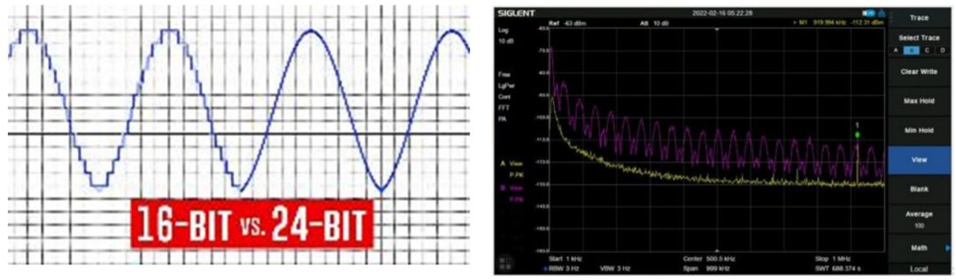
Figure 1. Power Supply Quality vs Effective Bits vs Effective Bandwidth
ADI has launched the solution “Power Management Selection for Signal Chains – Maintaining All Required Accuracy in Design”, which details various power supply architectures and their characteristics while analyzing the adaptability of power supply selection based on practical case requirements. Scan the code to download~

Scan to Download the Latest Solutions
[ADI Power Management Selection for Signal Chains – Maintaining All Required Accuracy in Design]
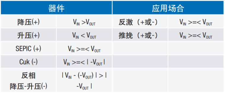
From the perspective of whether the signal is isolated, converters can be divided into non-isolated and isolated types. Table 1 illustrates common types of converters. Different circuit types have different conversion characteristics, and node noise varies accordingly. Non-isolated topologies mainly consist of inductors, switching devices, and capacitors; isolated topologies mainly consist of transformers, switching devices, and capacitors.
LDOs are linear converters and are not included in the following topology types. For applications where the load current is small, such as several or dozens of mA, and the input voltage difference exceeds the maximum supply rail, LDOs will be used, but LDOs cannot generate negative voltage rails. At low frequencies, LDOs have good noise performance.
Table 1. Overview of Converter Topologies
Buck converters always have VIN greater than VOUT. Due to the minimum duty cycle limitation, it is impossible to achieve large voltage difference conversions at a given operating frequency, such as converting 50V to 1V.
As shown in Figure 2, different colors indicate the current paths generated by the switching devices turning on and off, with different colors representing several loops, marked in red, blue, orange, and green:
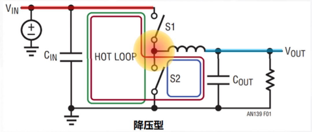
Figure 2. Buck Converter
-
Red Loop: The current path when controlling the switching device S1 to turn on. The input end is in series with the switch, making it a high noise node;
-
Blue Loop: The current path when controlling the switching device S1 to turn off and switching device S2 to turn on. The output end is in series with the second-order LC filter, making this node noise relatively low;
-
Orange Node: The high-frequency switching of switching devices S1 and S2 causes this node to produce high-frequency voltage alternating changes, thus generating high-frequency radiation. PCB layout should keep the size as small as possible;
-
Green Loop: This loop is generally called the thermal loop, also known as the high di/dt loop. For buck converters, its input side is the thermal loop. This loop has rapidly changing current edges, and the edge transitions in the time domain correspond to a wide spectrum in the frequency domain. Therefore, to avoid high-frequency noise, the physical size of this loop should be minimized during PCB layout.
Application scenarios for buck converters include:
-
Wide input range;
-
System efficiency requirements significantly greater than what LDOs can provide;
-
System requires clean output.
For internally compensated buck devices, compensating when the duty cycle is much greater than 50% can be tricky, while we also want to avoid low-frequency oscillations.
Recommended Models
-
LT8618: 65VIN/100mA, small size, synchronous
-
LT8604C: 42VIN/120mA, small size, synchronous
-
MAX17530: 42VIN/25mA, ultra-small device, wide input voltage range, synchronous
-
LT8609S: 42VIN/2A, unique Silent Switcher 2 architecture
LT8618, LT8604C can be directly ordered from the ADI China online store.
In a boost converter, VIN is always less than VOUT. Due to maximum duty cycle limitations, users cannot obtain any desired high voltage.
As shown in Figure 3, the boost topology has S2 as the control switch, which is similar to the buck topology, appearing as a flip on the X-axis. The input end is in series with the LC filter, making the input node a quiet node, while the output end is in series with the switch, thus generating conducted noise.
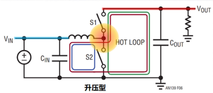
Figure 3. Boost Converter
Generally, a boost converter is chosen when the voltage required by the load is higher than the input voltage or when a higher intermediate bus voltage is desired. When designing boost circuits, the output thermal loop size should be minimized to reduce radiated noise. Additionally, attention should be paid to the feedback node, as the output voltage generated by feedback can be high enough to damage the switch and any downstream devices. If the feedback node is shorted, the circuit will be affected by destructive voltages.
Recommended Models
-
LT8330: 60V/1A (switch), small size, non-synchronous boost converter
-
LT3461: 40V/250mA (switch), small size, integrated Schottky diode
-
LT8410: 42V/25mA (switch), ultra-small size, synchronous boost converter
-
LT8338: 40V/1.2A (switch), small size, synchronous boost converter
LT8330, LT3461, LT8410, LT8338 can be directly ordered from the ADI China online store.
Due to space constraints, the introduction and model recommendations for the above converters can be found in the solution “Power Management Selection for Signal Chains – Maintaining All Required Accuracy in Design” for the complete document.

Scan to Download
The flyback is based on the boost topology, with the difference being that isolation is achieved through a transformer. The duty cycle constraints change, and the duty cycle is proportional to the winding ratio, allowing for almost any VIN/VOUT ratio to be obtained.
As shown in Figure 7, the flyback has two thermal loops, one at the input and one at the output, which need to be minimized. The size of the transformer can sometimes make this task challenging. The switching node generates large flyback pulses, which are proportional to the output current and require a regulation network for buffering, and these components can sometimes also radiate.
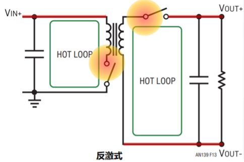
Figure 7. Flyback Converter
The flyback can be used when DC isolation is required between the backplane and the thermal side, for field or instrumentation control. The flyback can also be used when isolation is needed, but the input-output range must be relatively wide, for example, generating hundreds or thousands of volts. This topology often has higher common-mode leakage currents, so caution is needed when used in systems with safety standard ratings.
Since the output pulses have no inherent connection, any node can be secondary, even with multiple polarities with additional windings. Also, non-optical feedback devices tend to have more gentle voltage and load regulation than direct feedback.
Recommended Models
-
LT8301: Non-optical/Single-chip, 42V/6W
-
LT3511: Non-optical/Single-chip, 100V/2.5W
-
LTC3803: Non-optical/Controller, 75V/15W
-
LT3001: Non-optical/Single-chip, 36V/4W
LT8301, LT3511, LTC3803, LT3001 can be directly ordered from the ADI China online store.
Like the flyback topology, the push-pull topology also uses a transformer to adjust the output, but the operation of this topology limits its maximum duty cycle to 50%.
As shown in Figure 8, the push-pull topology has two switching nodes, with an LC filter in series with the output on the secondary side, making this topology very useful when a quiet output is needed, which makes it popular in signal chain applications that require isolation. The input side has a thermal loop, and the simplified model shows the cyclical thermal loop, with each conduction time being half, so the thermal loop is essentially a superposition of two half-cycle loops.
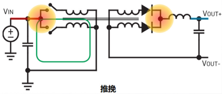
Figure 8. Push-Pull Converter
When DC isolation is required while wanting to reduce output noise and common-mode leakage current, the push-pull structure is typically chosen. Considerations related to this topology include duty cycle limitations; if the bus changes, it may cause offsets on the secondary side, and the duty cycle clamp is at 50%. Additionally, transformers used for this topology can sometimes be larger, and compared to flyback circuits that transmit the same amount of power, push-pull circuits have lower common-mode leakage currents.
Recommended Models:
-
LT3999: Programmable current limit, Fsync up to 1MHz, 2.7V-36VIN/Dual-channel 1A (switch)
-
MAX13253: Low noise controlled slew rate, 250/600KHz, with spread spectrum, 3.0V/5.5VIN/Dual-channel 1A (switch)
-
MAX256: Simple low noise isolation, 3.3V/5VIN – 3W
LT3999 can be directly ordered from the ADI China online store.
Due to limited space, the introduction and model recommendations for the 4 switch buck-boost converter can be found in the solution “Power Management Selection for Signal Chains – Maintaining All Required Accuracy in Design” for the complete document.

Scan to Download
After understanding the basic conversion types and the relationship between noise and input and output, it is necessary to consider how to flexibly apply, integrate, and establish a complete power system in the system. The general approach is to draw a system diagram, also known as a power tree, and systematically decompose and analyze to determine the rationality of the power supply scheme.
When establishing a power tree, it is necessary to determine the characteristics of the system’s input voltage, whether it is fixed input or has a wide input range? It is also necessary to determine the power characteristics required by the system signal chain, whether it requires positive or negative voltage? What is the current consumption? What is the expected noise level and the highest accuracy needed in the signal chain?
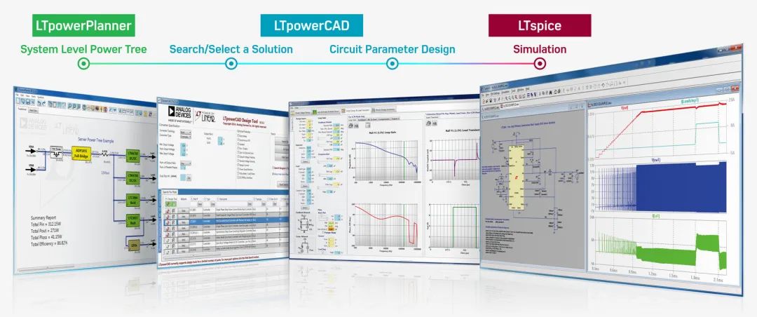
ADI provides the design tool Power CAD to assist users in hypothesis analysis and iterative design, helping to provide reasonable power supply solutions.
The solution “Power Management Selection for Signal Chains – Maintaining All Required Accuracy in Design” shares 2 case studies, Case Study 1 examines the noise characteristics of converters, such as charge pumps having high noise at both the input and output; it also clarifies design priorities, for instance, although buck converters have higher efficiency, for applications with power consumption of only a few milliamps, the efficiency difference does not translate to much heat, making LDOs more suitable. Case Study 2 focuses on noise, thus requiring the use of LDOs, while also needing boost, hence choosing LDO and boost converters to achieve the lowest output noise. However, the downside is that this solution uses 3 boost converters and 4 LDOs.
……
For complete case studies and analysis, please scan the code to download the solution “Power Management Selection for Signal Chains – Maintaining All Required Accuracy in Design” for viewing.

Scan to Download the Latest Solution
[ADI Power Management Selection for Signal Chains – Maintaining All Required Accuracy in Design]