
Even in power-dominant events such as wireless connectivity in Internet of Things (IoT) applications, allowing as many processes to run autonomously can significantly enhance battery life. Reducing power consumption has always been a major focus in the microcontroller (MCU) market. Ultra-low power MCUs can now greatly reduce power consumption in both active and deep sleep modes. The effects of this change are evident, greatly improving battery life in our daily embedded applications and providing the possibility of using energy harvesting in the future.
However, to reduce power consumption based on new MCUs, developers must consider many factors. Silicon Labs has specifically written a technical article titled: “Running Your Embedded System at 0 MIPS” to help developers understand how to leverage the autonomous operation of peripherals in new MCUs to achieve the low power promised in the datasheet by operating closer to “0” MIPS.
Low Power is Key to Embedded System Development
For new MCUs and wireless MCUs (WMCUs) used in power-sensitive IoT applications, the power consumption during code execution has significantly decreased, even reaching below 40μA/MHz. With these low-power specifications, you might wonder why we need sleep modes, why not run your code at 500 kHz to achieve a current consumption of 20μA, allowing your application to run on battery for 10 years? The reality is not that simple.
Power consumption in sleep modes has also seen significant improvements over the past few years. We can now see power consumption in deep sleep modes below 2μA, with some sleep modes even below 50nA. You might think that having systems designed with these modes naturally results in low power consumption; however, the key is whether the application can utilize sleep modes.
Why is Active Mode Both Good and Bad?
The most straightforward way to use an MCU or WMCU is to let the CPU manage everything. For example, you can start an analog-to-digital converter (ADC), place some data into a communication interface (like USART transmission), read the ADC data, and process the data, all directly controlled by the CPU. Direct CPU control simplifies development, but the cost is that whenever a peripheral or external event needs to be handled, the MCU will be in active mode, significantly increasing power consumption.
Recently, some datasheets show that the current in active mode is 40μA/MHz or even lower, which is usually the parameter at high clock frequencies, increasing at lower frequencies, leading to greater absolute power consumption. This is because the relationship between frequency and power consumption in active mode is not linear. Power consumption consists of two parts, where the second part is not closely related to frequency:
1. The processor itself, which varies proportionally with frequency.
2. Modules with a baseline operating current, such as low-dropout regulators (LDOs), brown-out detectors (BODs), etc.
To reduce power consumption, it is essential to minimize the time the MCU operates in high-power active mode, turn off peripherals whenever possible, and allow the CPU to sleep as much as possible.
Power Budget
For battery-powered applications constrained by energy, knowing where energy is consumed is crucial for optimization. Table 1 shows a power budget for a sensor-detecting wireless application, which is not well optimized.
Power consumption can be measured or estimated by averaging the power consumption of each component. If the CPU duty cycle is two percent and operates at 60μA/MHz at 20 MHz, the CPU consumption would be 24μA.
Note that the power budget shown in Table 1 is categorized by function. For example, the baseline sleep current includes a low-frequency oscillator and a real-time clock (RTC) to time system events, allowing for deep sleep.
The sensor measurement part is triggered by a 0.5kHz interrupt, with deep sleep between interrupts. Low-power Bluetooth sends data every second, which is a common low-power application. Finally, there is some power consumption from non-MCU parts. The MCU may not directly control some of these modules, including power management peripherals. In this example, the MCU directly controls the ADC to sample the sensor; otherwise, the sensor current would be entirely based on the data shown.
For this example, the continuous current of the sensor is about 390μA, but by adjusting the duty cycle, each ADC sample only uses 10μs, significantly reducing power consumption.
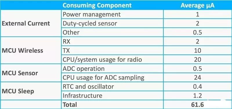
Table 1 Power Budget for Target Application
If this wireless application is powered by a CR2032 battery with a capacity of 225 mAh, its lifespan at an operating power of 61.6μA would be approximately 0.4 years. In fact, we can do better.
Improving the Status Quo
Let’s look at ways to reduce the MCU sensor measurement current. Although this example involves ADC measurements of external sensors, related examples may focus on a range of different types of measurements and interactions with the external environment. In both cases, there will be frequent interactions between the MCU and the external environment.
The simplest way to achieve low-power sensing is to keep the CPU in sleep mode as much as possible, waking it only during sampling and returning to sleep mode as quickly as possible. This method works well for very low sampling rates, but as shown in Figure 1, as the number of samples per second increases, the system’s power consumption also significantly increases:
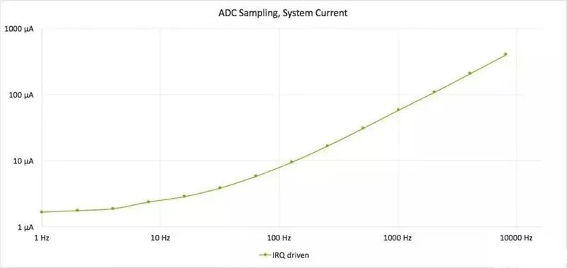
Figure 1 ADC Sampling Current
Using interrupts for ADC sampling shows that as the number of samples per second increases, power consumption also increases. Many types of applications must have frequent activity while still maintaining battery life. An activity rate exceeding 1kHz is not unheard of, at which point measures must be taken to maintain low power consumption.
Figure 2 shows two additional methods for sensor management. The Peripheral Reflex System/Direct Memory Access (PRS/DMA) method allows the CPU to perform ADC sampling in deep sleep mode without any involvement. Instead of the RTC waking the CPU, which then starts the ADC for sampling, the RTC sends events directly to the ADC through the event system (such as Silicon Labs’ PRS). The ADC automatically starts the ADC conversion upon receiving this event. Once the conversion is complete, the DMA can also operate from deep sleep mode, retrieving data from the ADC and storing it in RAM. The benefit of the PRS/DMA method is a significant reduction in current consumption. At 1 kHz, the system current drops from 58μA to 25μA.
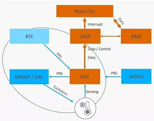
Figure 2 This ADC Sampling Graph Shows Power Consumption Under Various Operating Modes
A more efficient way to drive the ADC is the PRS/Comparator (CMP) method, where the RTC still triggers the ADC through the PRS system, but in this case, the ADC immediately evaluates the samples using the comparator function, and DMA or CPU is not used unless necessary data is found. This method can achieve a system current of only 3.5μA at a 1 kHz sampling rate.
Dynamic ADC Comparator
Using the PRS/CMP method, most sampling data is discarded, and the CPU only focuses on the data that needs processing. This method is effective when the signal changes slowly or when specific signals are needed.
When using the comparator function to monitor signals, one approach is to measure the signal and set a threshold based on this signal. As long as the signal remains within the threshold range, the system can remain in deep sleep mode, with the CPU also kept in sleep mode.
However, if the signal changes and exceeds the threshold, the system will recognize this signal and take appropriate action. Before returning to sleep mode, the ADC threshold will be reconfigured to accommodate the new signal value, allowing the system to enter sleep mode again until the next signal change. Figure 3 illustrates an example of this technique. The dots represent ADC samples, and the arrows indicate that whenever the CPU is awakened, it will record this change and reconfigure the threshold.
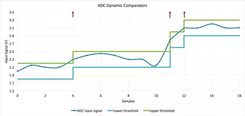
Figure 3 When the Signal Exceeds the Threshold, the CPU Interrupts Dynamically Modifying the ADC Threshold
Using this method, the system will actually lose some signal accuracy because the signal can move arbitrarily within the threshold range between triggers. However, the benefit is a significant reduction in power consumption.
If the goal of the system is to measure the dynamic value of the signal, the PRS/DMA-driven method is ideal, as it makes all data available while still providing very beneficial energy-saving features.
Autonomous Working Subsystems
The ADC example is just one of many ways to reduce application power consumption through sleep modes. New MCUs focused on low-power applications (such as Silicon Labs’ EFM32 Gecko MCU) have a wealth of features that can operate in deep sleep mode, enabling a high level of autonomous behavior.
For example, the Gecko MCU’s LESENSE (Low Energy Sensing) module can automatically and periodically sample up to 16 channels without any CPU involvement. It can achieve high-frequency detection and operate for 10 years on a single charge.
In many cases, a single peripheral can autonomously fulfill its duties, but there are also many situations that require interaction. In such cases, we can leverage peripheral interconnects like the PRS system present in some of the current new MCUs. These peripheral interconnects allow multiple peripherals to connect to autonomously perform more complex tasks.
Figure 4 shows an example of such an autonomous system that uses an event chain to perform its functions:
1. The RTC periodically sends a PRS signal to the ADC to initiate conversion at a given time.
2. The RTC simultaneously activates the external sensor, so the signal is ready when measuring.
3. The ADC completes the sampling and notifies the DMA, which transfers the data to RAM.
4. The completion PRS signal from the ADC turns off the external sensor.
5. The CPU is awakened by an interrupt when the buffer is full or when the ADC threshold is exceeded.
6. Optional: The PRS watchdog monitors the event loop to ensure it continues to run.
The DMA can take over from the system shown in Figure 4 by setting the ADC’s comparator function to be more power-efficient.
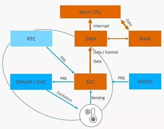
Figure 4 This Autonomous ADC System Includes Periodically Operating Sensors and a Watchdog
These autonomous subsystems have several key advantages:
1. Significant energy savings.
2. Sensors can continue to operate stably even under heavy CPU load.
The downside is that not all MCUs support this type of operation, and when setting up interactions, you will want to think like a hardware designer. Overall, for many battery-powered applications, the advantages clearly outweigh the disadvantages.
Conclusion
By leveraging various energy-saving techniques, the CPU is almost entirely disengaged from work when the sensor is measuring. For the wireless application shown in Table 1, this will reduce the total average power consumption from 61.6μA to 37.6μA, a reduction of 39%, extending battery life from approximately 5 months to 8 months, an increase of 64%, or allowing for a reduction in battery size to improve system form factor.
For non-wireless applications, energy savings will be even more significant. In the example in Table 1, energy consumption will drop from 29.6μA to 5.6μA, powered by a CR2032 battery, theoretically extending lifespan from 10 months to 4.6 years.


1. A pictorial guide to understanding the STM32 clock
2. With so many embedded operating systems, which one is right for you?
3. A must-read book list for Android developers
4. More important than choosing an operating system is making good use of the chosen operating system!
5. A shared learning framework for C language in microcontrollers
6. 6 commonly used sensors, do you know their principles?

Disclaimer: This article is a network reprint, and the copyright belongs to the original author. If there are any copyright issues, please contact us, and we will confirm the copyright based on the copyright certificate you provide and pay for the manuscript or delete the content.