This article is reprinted from the Extreme Technology CommunityExtreme Technology Column: Arm Technology BlogSource: Helium Technology Lecture | The Power of Sudoku, Registers, and Belief
As artificial intelligence (AI) permeates various applications, the largest number of IoT devices in the market will also be endowed with intelligence. The Arm® Helium™ technology brings critical performance enhancements for machine learning and digital signal processing to devices based on Arm Cortex®-M processors.
In last week’s Helium Technology Lecture, participants learned about the core “pipelined” execution of Helium technology. Today, we will explore some complex and interesting interleaved load/store instructions. If you want to learn how to efficiently utilize Helium, don’t miss the video at the end, where Arm technology experts demonstrate how Helium introduces more intelligence to endpoint devices.
The Origin of Arm Helium Technology
The Power of Sudoku, Registers, and Belief
Author: Thomas Grocutt, Chief Architect and Researcher of the Arm Architecture and Technology Division M Series
An important part of DSP processing is the efficient handling of different data formats, which often need to be transformed into different arrangements for computation. Image data is a good example, as it is typically stored in an interleaved stream of red, green, blue, and alpha pixel values. However, to vectorize the computation, all red pixels need to be placed in one vector, green pixels in another, and so on. In the Neon architecture, the VLD4/VST4 instructions can perform this transformation, as shown in the figure below.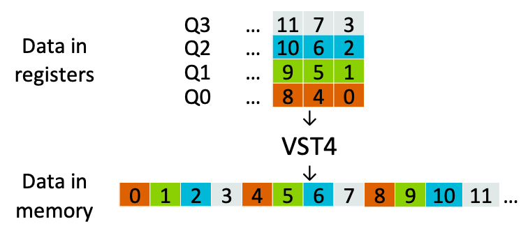 VST4 interleaves four 128-bit registers, storing a total of 512 bits of data. The Neon architecture supports various interleaving/de-interleaving operations for different formats. For example, the provided VST2 can be used to interleave the left and right channels of stereo audio. These instructions also support element sizes ranging from 8 to 32 bits.One of the main advantages of MVE’s “pipelined” execution is that it allows memory and ALU operations to overlap, even in a single-issue processor. As shown in the figure below, to achieve double performance based on this technology, all instructions must perform the same workload.
 It is evident that the performance gains from overlapping will be significantly reduced by wide storage instructions like VST4. The solution provided by MVE is to partition the storage space into blocks that balance with ALU operations, with each block storing 128 bits of data. MVE allows for four-way interleaving composed of the four instructions VST40, VST41, VST42, and VST43. However, this is not the end; many issues still exist:
-
The obvious splitting method is to have the four instructions store different data streams (e.g., VST40 stores all red pixels, VST41 stores green pixels, etc.). For 8-bit pixel data, this means each instruction will store 16 non-contiguous bytes. This access pattern is very complex for the memory subsystem and can lead to significant stalls. Instead, the instructions need to generate large contiguous requests.
-
To correctly coordinate with other vector instructions, the register file ports must be set to access the rows of the register file (i.e., the entire vector register) rather than the columns (i.e., the first byte of the four registers); if data is to be interleaved and stored in contiguous memory blocks, column access is required.
-
To avoid the timing crossing issues I described in the previous content, we need to split the instructions into several “pulses”, first reading the [63:0] bits of the register, and then reading the [127:64] bits in the next cycle.
-
The solution must work for both two-way and four-way interleaving, as well as for 8, 16, and 32-bit data operations.
Faced with all these conflicting constraints, we feel like we’ve fallen down a rabbit hole, and I can’t help but recall a scene from “Alice in Wonderland”:
Alice: This is impossible. Mad Hatter: As long as you believe, anything is possible.
So, let us set aside our doubts for a moment and take a closer look at the read ports to see what happens.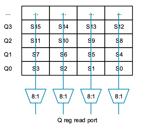 MVE reuses the floating-point register file, so the vector registers (Q0 to Q7) are composed of several groups of “S” registers, each grouped by four. Each column multiplexer selects the same row and then merges the data to access the entire Q register (see the figure above). However, what if we cannot select from any register in a column, but instead distort the ports to select from registers in alternating columns, as shown in the figure below:
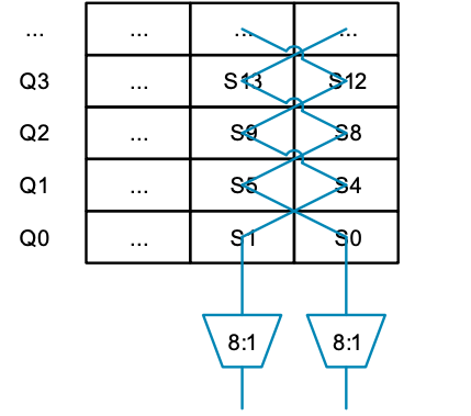 If the control inputs on the 8:1 multiplexer are set to the same value, a row of data can be read (e.g., S0 and S1). However, if different values are used, a pair of values can be read from a column (like S0 and S4). Now it seems feasible; we can read data from both columns and rows. If we enlarge the bottom of the figure and replace the register numbers with the numbers of the multiplexers they are connected to, we get the following result:
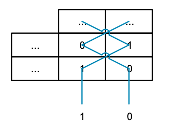 This is similar to a simple Sudoku puzzle, where each number appears only once in each row and column of the repeated matrix, except this matrix is 2 x 2 instead of the usual 9 x 9. Since we can only read two values from a column and can only handle 32-bit values (the width of the multiplexer), this pattern can only provide a two-way interleaving solution. Since we need a pattern that can handle all interleaving modes and data width combinations, it is conceivable to vertically stack all combinations to create a multi-resolution three-dimensional Sudoku puzzle. Solving one layer of the puzzle is easy, but solving the entire three-dimensional puzzle must be breathtaking. Additionally, we need to consider the other limiting factors mentioned above, such as contiguous memory access and splitting access to the upper and lower 64 bits of the registers across different cycles.After some thought, I realized that the problem could be divided into two parts: first, to determine a method to represent all constraints in a single unified problem space, and second, to solve these constraints with a monotonic task. Since this pattern resembles a very complex Sudoku problem, and many Sudoku programs are based on SAT solvers, I had the idea of using a SAT solver to complete the monotonic constraint-solving task. After some effort, I devised a method to represent all constraints, and after debugging, the first feasible solution was born. Although it is not perfect and leads to complex control logic for the multiplexer, at least victory is in sight. Not wanting to manually clean up the solution, we added some additional constraints, introduced some symmetry, and produced the final solution, which turned out to be a pair of doubly nested quadruple helical structures:
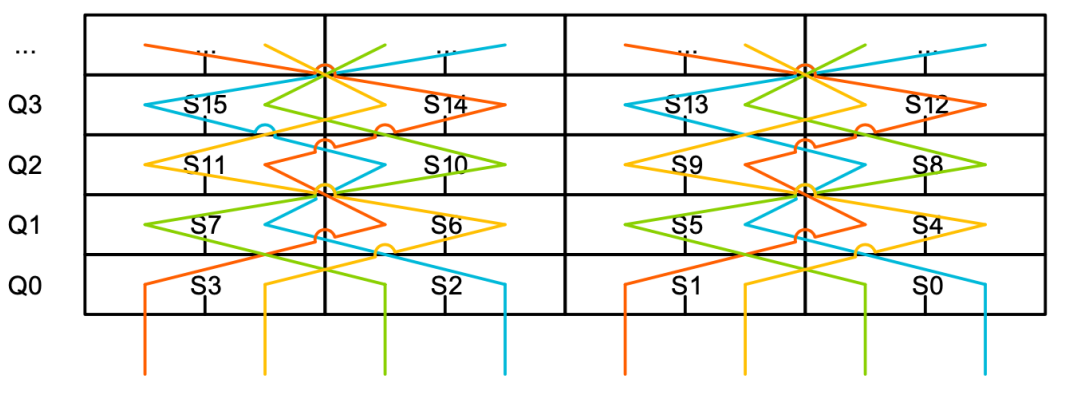 To show everyone the nested helical lines, I marked the path of a single multiplexer in the figure below. As shown, the path alternates through the 32-bit “S” registers (as shown on the left), and every two rows swap through the upper and lower halves of the 16-bit regions of the “S” registers (as shown on the right).
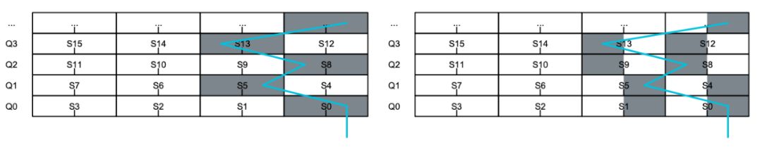 Intuition tells me that this distortion method will not work for three-way interleaving, and I was proven right; the SAT solver formally proved it to be unsolvable.This distortion method means that data can be accessed simultaneously from both rows and columns of the register file. However, the problem is that the bytes returned by the read ports may be out of order, and the order depends on the accessed registers. To correct this situation, a cross multiplexer is needed to swap everything back to the correct position. Since other instructions like VREV and complex native operation instructions will use the cross multiplexer, we can use it for free. This confirms the saying: “If you must use a piece of hardware, make the most of it.”The figure below shows some instruction access patterns derived from the read port distortion mode. The first case (VST2n.S32) shows reading 32 bits (S32) from vector registers Q0 and Q1 and interleaving them (like left and right audio channels). The colors in the figure represent the portions of the registers read by the two instructions (i.e., VST20 reads the orange portion), and the text in the elements indicates the byte offsets stored in memory.
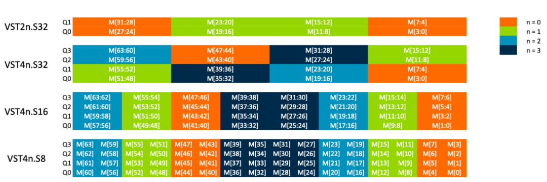 It can be seen that the S8 and S16 modes place the same data in the same color regions of the registers; the only difference is the arrangement of bytes within each section. This means that with different configurations in the cross multiplexer, the 16-bit mode can also support 8-bit. These modes are also applicable to the write ports used by load instructions. In addition to establishing register file ports, these modes also mean that memory access is always a pair of contiguous 64-bit blocks, which can improve memory access efficiency. Furthermore, the [3] bit of the addresses of these data blocks is always different, allowing for parallel transmission on systems with two sets of interleaved 64-bit memory.The research team has accumulated two important experiences from these instructions. First, to achieve breakthrough progress in gate count and efficiency, architectural design must be synchronized with micro-architectural details. Second, one must maintain faith and believe that anything is possible.Do you want to learn more about Helium technology? A Helium technology video has been recorded by Mark Quartermain, Technical Director of Arm’s IoT Division, and Matthias Hertel, Senior Manager of Embedded Tool Integration at Arm’s IoT Division, demonstrating how to efficiently utilize Helium through practical examples.In the next Helium article, we will continue to explore related topics on memory access and introduce some technical knowledge for implementing circular buffers. Stay tuned for the Helium Technology Lecture, and see you next time!Recommended Reading:
- Helium Technology Lecture | Why Not Directly Use Neon?
- ARM Hint Instruction – Detailed Explanation of WFI (Wait For Interrupt) Instruction
- Arm Expands Cortex-M Product Line, Bringing AI to Ultra-Small Endpoint Devices
Reprinted from | Extreme Technology Community
Copyright belongs to the original author. If there is any infringement, please contact for deletion.
END


关于安芯教育


安芯教育是聚焦AIoT(人工智能+物联网)的创新教育平台,提供从中小学到高等院校的贯通式AIoT教育解决方案。
安芯教育依托Arm技术,开发了ASC(Arm智能互联)课程及人才培养体系。已广泛应用于高等院校产学研合作及中小学STEM教育,致力于为学校和企业培养适应时代需求的智能互联领域人才。