The groundbreaking Intel 8008 microprocessor was first produced over 50 years ago. It was Intel’s first 8-bit microprocessor and is the ancestor of the x86 processor series you may be using today. I couldn’t find a good die photo of the 8008, so I opened one and took some detailed photos. This article includes these new chip photos and a discussion of the internal design of the 8008.
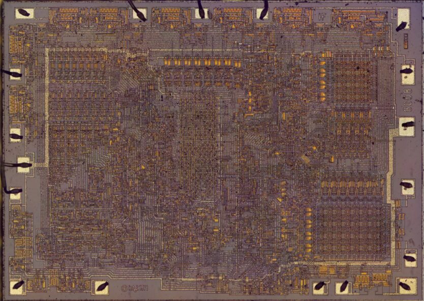
The image below shows the micro silicon chip inside the 8008 package (click to view a higher resolution photo). You can barely see the wires and transistors that make up the chip. The squares around the outside are 18 pads connected to external pins through tiny bonding wires.
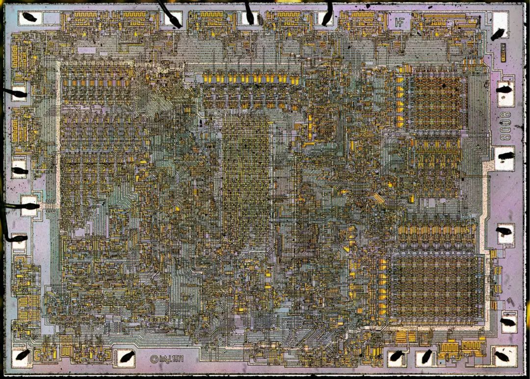
You can see the text “8008” on the right edge of the chip, and “© Intel 1971” on the bottom edge. The initials HF of Hal Feeney appear in the upper right corner, who was responsible for the chip’s logic design and physical layout. Other key designers of the 8008 include Ted Hoff, Stan Mazor, and Federico Faggin.
Inside the Chip
The image below highlights some of the main functional blocks of the chip. On the left is the 8-bit Arithmetic/Logic Unit (ALU), which performs the actual data calculations.
The ALU uses two temporary registers to hold its input values. These registers take up a large area on the chip, not because they are complex, but because they require large transistors to drive signals through the ALU circuitry.
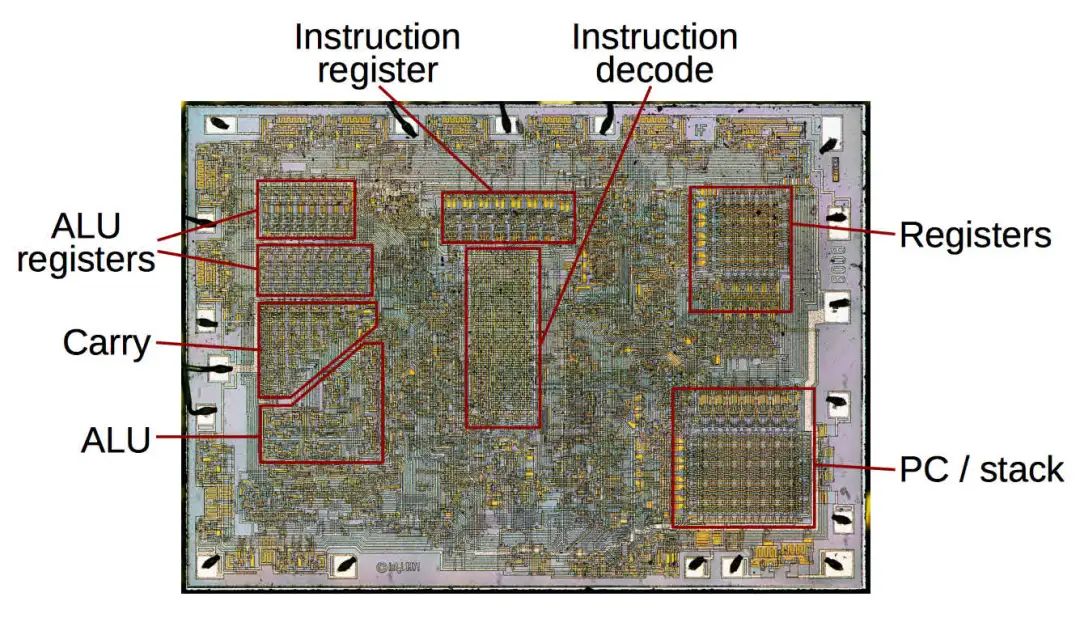
Below the registers is the carry look-ahead circuitry. For addition and subtraction, this circuitry calculates all eight carry values in parallel to improve performance. Since the low-order carry only depends on the low-order bits, while the high-order carry depends on multiple bits, the circuit block has a triangular shape.
The triangular layout of the ALU is quite unusual. Most processors stack the circuitry for each bit into a regular rectangle (a bit-slice layout). However, the 8008 has eight blocks (one for each bit) arranged randomly to fit the space left by the triangular carry generator. The ALU supports eight simple operations.
At the center of the chip is the instruction register and instruction decoding logic, which determines the meaning of each 8-bit machine instruction. Decoding is done using a Programmable Logic Array (PLA), which is an arrangement of gates that can match bit patterns and generate appropriate control signals for the rest of the chip. On the right side is the storage block. The 8008 has seven registers located in the upper right corner. The lower right corner is the address stack, consisting of eight 14-bit address words. Unlike most processors, the 8008’s call stack is stored on the chip rather than in memory. The program counter is just one of these addresses, making subroutine calls and returns very simple. The 8008 uses dynamic memory for storage.
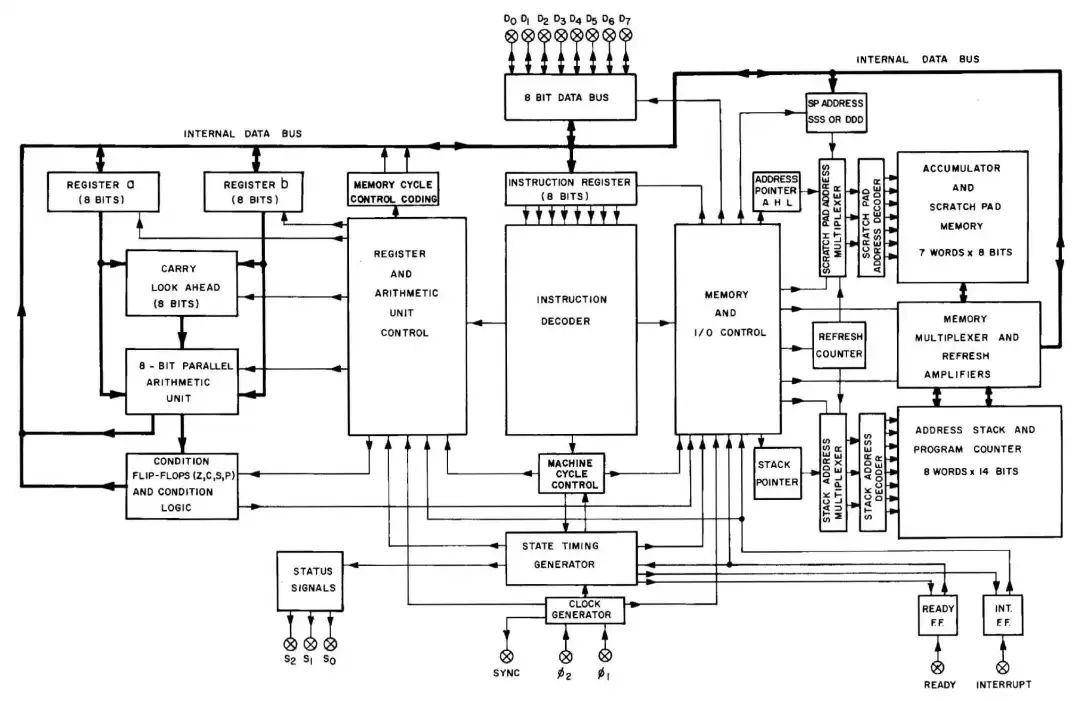
The physical structure of the chip closely resembles the block diagram in the 8008 user manual (shown below), with the block positions on the chip almost identical to those in the block diagram.
Chip Structure
What do die photos show? For our purposes, the chip can be viewed as three layers. The image below shows a close-up of the chip, indicating these layers. The top layer is the metal wiring. This is the most obvious feature, looking metallic (not surprisingly). In the detailed view below, these wires are mostly horizontal. The polysilicon layer is located beneath the metal and appears orange under a microscope.
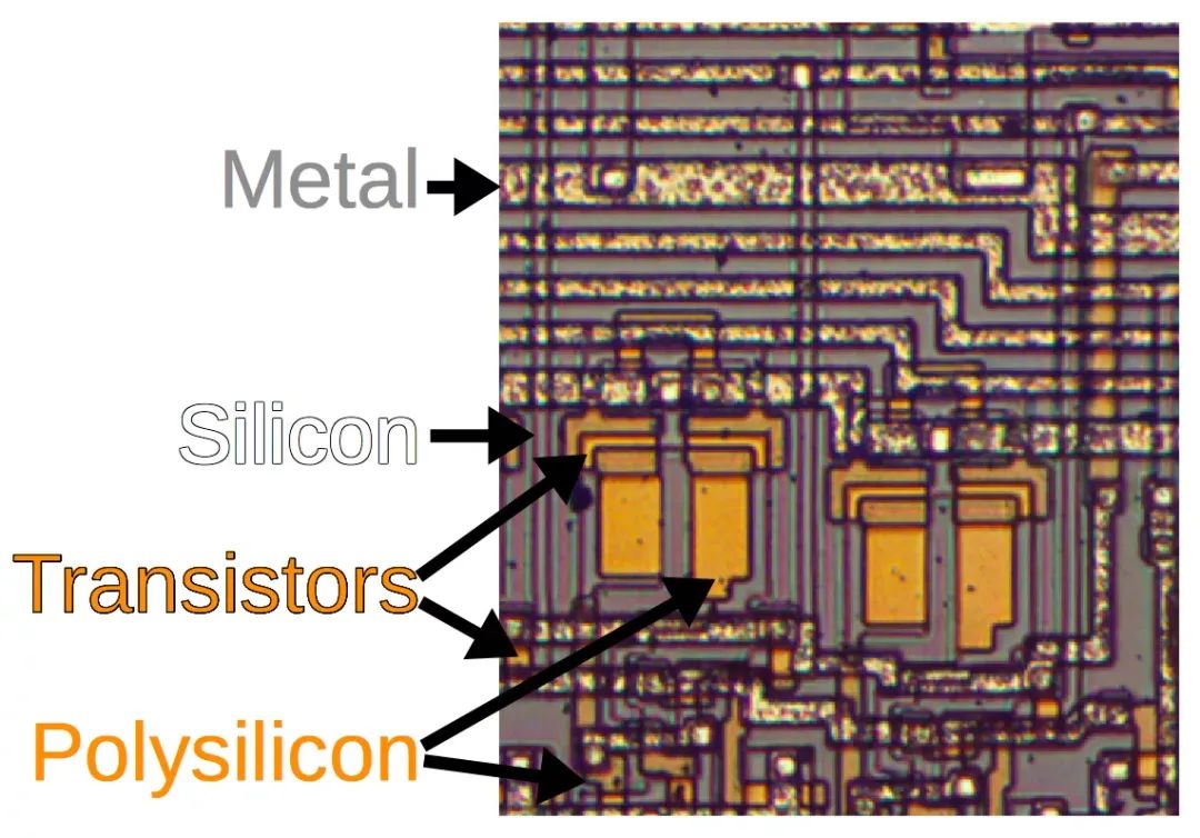
The base of the chip is the silicon wafer, which appears purple-gray in the photo. Pure silicon is actually an insulator. Certain areas are “doped” with impurities to form semiconductor silicon. The silicon layer is at the bottom and difficult to distinguish, but black lines can be seen at the boundary between doped and undoped silicon. Some vertical silicon “lines” can be seen in the photo.
The transistors are the key components of the chip, where the polysilicon lines intersect with the doped silicon to form transistors. In the photo, the polysilicon appears brighter orange when forming transistors.
Why an 18-Pin Chip?
One inconvenient feature of the 8008 is that it has only 18 pins, which makes the chip slower and harder to use. The 8008 uses 14 address bits and 8 data bits, resulting in 18 pins, which is not enough for each signal. Instead, the chip has 8 data pins that are reused over three cycles to transmit low address bits, high address bits, and data bits. Computers using the 8008 require many supporting chips to interact with this inconvenient bus architecture.
There was no compelling reason to force the chip to be 18 pins. 40 or 48 pin packages were common among other manufacturers, but 16 pins were “Intel’s belief.” They were extremely reluctant to switch to 18 pins. Years later, when the 8080 processor was introduced, Intel had accepted the 40-pin chip. The 8080 was more popular, partly because it had a simpler bus design allowed by its 40-pin package.
Power and Data Paths in the Chip
The data bus provides the data flow through the chip. The image below shows the 8-bit data bus of the 8008, with 8 data lines in rainbow colors. The data bus connects to the 8 data pins on the outer half of the upper part of the chip. The bus runs between the ALU on the left, the instruction register (top center), and the registers and stack on the right. The bus separates on the left, with each half occupied by the ALU.
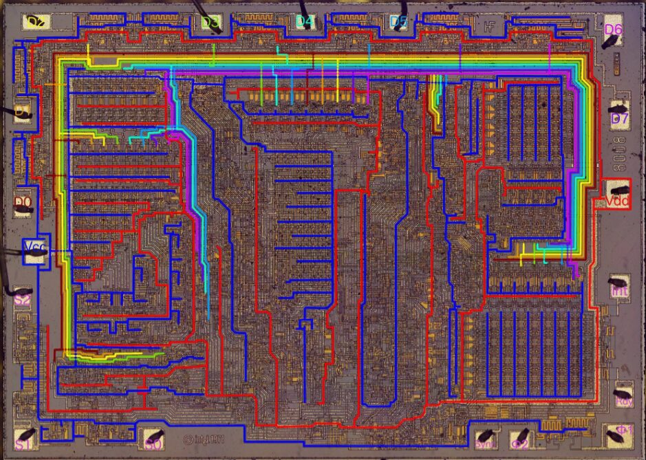
The red and blue lines show the power wiring. Power wiring is an often-overlooked aspect of microprocessors. Power is wired in the metal layer due to its low resistance. However, since early microprocessors had only one metal layer, careful planning of power distribution was necessary to avoid path crossings. The image above shows the Vcc line in blue and the Vdd line in red. Power is supplied through the Vcc pin on the left and the Vdd pin on the right, then branches into thin interlocking wires to power all parts of the chip.
Register File
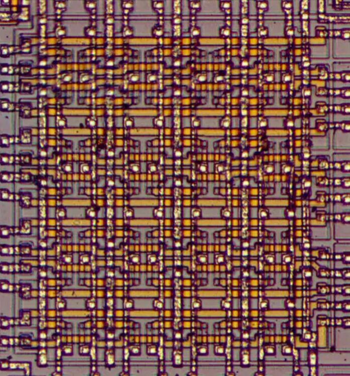
To showcase what the chip looks like in detail, I enlarged the register file of the 8008 in the image below. The register file consists of a grid of dynamic RAM (DRAM) storage cells arranged in 8 x 7, with each storage cell using three transistors to hold one bit. (You can think of the transistors as small rectangles, where the orange polysilicon appears slightly brighter.) Each row is one of the seven 8-bit registers of the 8008 (A, B, C, D, E, H, L). On the left, you can see seven pairs of horizontal lines: the read select lines and write select lines for each register. At the top, you can see 8 vertical wires used to read or write the contents of each bit, along with 5 thicker wires for providing Vcc. Using DRAM as registers (rather than the more common static latches) is an interesting choice. Since Intel was primarily a memory company at the time, I suspect they chose DRAM because of their expertise in that field.
How PMOS Works
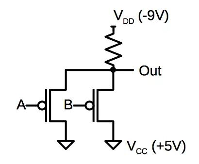
The 8008 uses PMOS transistors. To simplify a bit, you can think of a PMOS transistor as a switch between two silicon lines, controlled by a (polysilicon) gate input. When its gate input is low, the switch closes, and its output can be pulled high. If you are familiar with NMOS transistors used in processors like the 6502, PMOS may be a bit confusing, as everything is reversed.
A simple PMOS NAND gate can be constructed as follows. When both inputs are high, the transistor turns off, and the resistor pulls the output low. When any input is low, the transistor turns on, connecting the output to +5. Thus, this circuit implements a NAND gate. To be compatible with 5-volt TTL circuits, the PMOS gate (and the 8008) uses unusual voltage supplies: -9V and +5V.
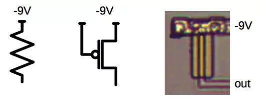
For technical reasons, the resistor is actually implemented using transistors. The image below shows how transistors are connected to act as a pull-down resistor. The details on the right show how this circuit appears on the chip. The -9V metal line is at the top, the transistor is in the middle, and the output is the silicon line at the bottom.
The History of the 8008
The complex story of the 8008 begins with the Datapoint 2200, a popular computer launched in 1970 as a programmable terminal. (Some consider the Datapoint 2200 to be the first personal computer.) The Datapoint 2200 did not use a microprocessor but contained a board-level CPU built from discrete TTL chips. (This was the standard way to build CPUs during the minicomputer era.) Datapoint and Intel decided that a single MOS chip could replace that board, and Intel launched the 8008 project to build the chip. Later, Texas Instruments (TI) also agreed to create a single-chip processor for Datapoint. Both chips were designed to be compatible with the 8-bit instruction set and architecture of the Datapoint 2200.
By around March 1971, Texas Instruments (TI) completed their processor chip, which they called the TMC 1795. After delays with the project, Intel completed the 8008 chip around the end of 1971. For various reasons, Datapoint rejected both microprocessors and built a faster CPU based on newer TTL chips (including the 74181 ALU chip).
TI attempted to market the TMC 1795 processor to companies like Ford but was unsuccessful and ultimately abandoned the processor to focus on more profitable calculator chips. On the other hand, Intel marketed the 8008 as a general-purpose microprocessor, which ultimately led to the x86 architecture you may be using today. While TI was the first to introduce an 8-bit processor, Intel made their chip successful, creating the microprocessor industry.
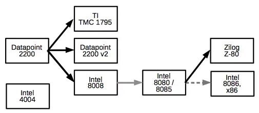
The image above summarizes the “genealogy” of the 8008 and some related processors. The architecture of the Datapoint 2200 was used for the TMC 1795, Intel 8008, and the next version of the Datapoint 2200. Thus, four completely different processors were built using the instruction set and architecture of the Datapoint 2200. The Intel 8080 processor is a significant improvement over the 8008. It significantly expanded the instruction set of the 8008 and reordered the machine code instructions for efficiency. The 8080 was used in groundbreaking early microcomputers such as the Altair and Imsai. After completing work on the 4004 and 8080, designers Federico Faggin and Masatoshi Shima left Intel to develop the Zilog Z-80 microprocessor, which improved upon the 8080 and became very popular.
The transition to the 16-bit 8086 processor was far less dramatic. Most 8080 assembly code could be converted to run on the 8086, but it was not straightforward due to the fundamental changes in the instruction set and architecture. Nevertheless, some features of the Datapoint 2200 still exist in today’s x86 processors. For example, the Datapoint 2200 had a serial processor that processed one bit at a time. Because it needed to process the least significant bit first, the Datapoint 2200 was little-endian. For compatibility, the 8008 is little-endian, and Intel’s processors still are. Another feature of the Datapoint 2200 was the parity flag, as parity calculations were very important for terminal communication. The parity flag has continued into the x86 architecture.
The 8008 was not architecturally related to Intel’s 4-bit 4004 processor. In any case, the 8008 was not an 8-bit version of the 4-bit 4004. The similar name was purely a marketing invention; during the design phase, the 8008 had a bland name, “1201.”
How the 8008 Fits into the History of Semiconductor Technology
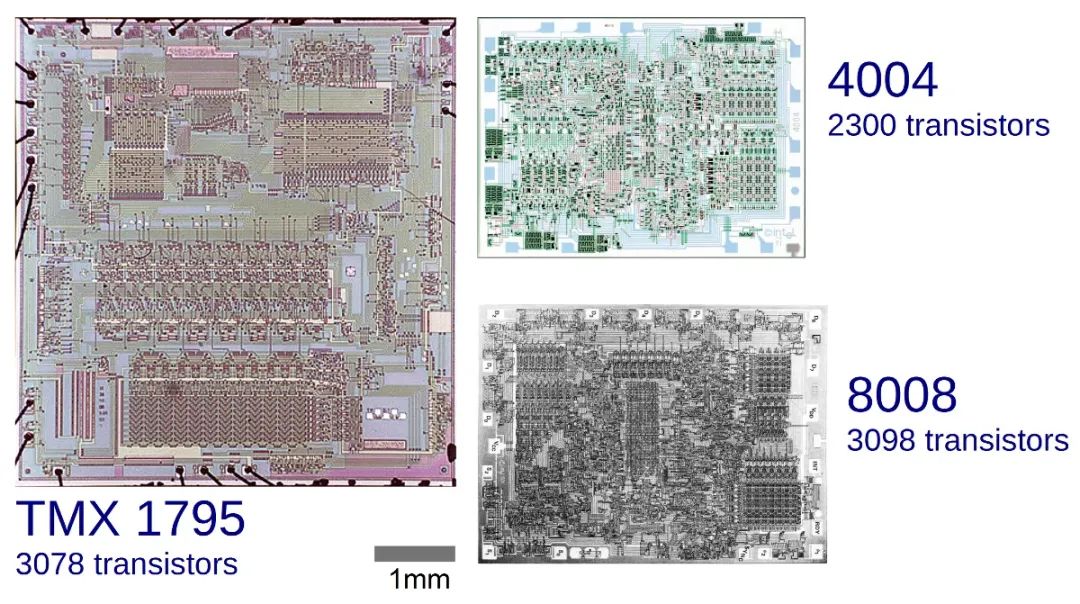
The 4004 and 8008 both used silicon-gate enhancement-mode PMOS, a semiconductor technology that was only briefly used. This places the chip at an interesting point in chip manufacturing technology.
The 8008 (and modern processors) use MOS transistors. These transistors had a long road to acceptance, being slower and less reliable than bipolar transistors used in most computers of the 1960s. By the late 1960s, MOS integrated circuits became increasingly common. The standard technology was PMOS transistors with metal gates. The gates of the transistors were made of metal and were also used to connect the chip’s components. The chip essentially had two functional layers: the silicon itself and the top metal wiring. This technology was used in many Texas Instruments calculator chips and in the TMC 1795 chip (which had the same instruction set as the 8008).
A key innovation that made the 8008 practical was the self-aligned gate—a transistor using polysilicon instead of a metal gate. While this technology was invented by Fairchild and Bell Labs, it was Intel that pushed this technology forward. The performance of polysilicon gate transistors is much better than that of metal gate transistors (for complex semiconductor reasons). Moreover, the addition of a polysilicon layer made signal wiring within the chip easier, allowing for denser chips. The image below shows the advantages of a self-aligned gate: the metal gate TMC 1795 is larger than the sum of the 4004 and 8008 chips.
Soon after, semiconductor technology advanced again, replacing PMOS transistors with NMOS transistors. Although PMOS transistors were initially easier to manufacture, NMOS transistors were faster, and once they could be reliably manufactured, they clearly won out.
NMOS gave rise to more powerful chips, such as the Intel 8080 and Motorola 6800 (both from 1974). Another technological improvement was changing the characteristics of transistors through ion implantation. This allowed for the creation of depletion-mode transistors that could serve as pull-up resistors. These transistors improved chip performance and reduced power consumption. They also allowed for the creation of chips that operated on standard five-volt power supplies.
The combination of NMOS transistors and depletion-mode pull-ups was used in most microprocessors from the late 1970s to the early 1980s, such as the 6502 (1975), Z-80 (1976), 68000 (1979), and Intel chips from the 8085 (1976) to the 80286 (1982).
By the mid-1980s, CMOS became dominant, using both NMOS and PMOS transistors to significantly reduce power consumption, with chips including the 80386 (1986), 68020 (1984), and ARM1 (1985). Almost all chips are now CMOS.
As you can see, the 1970s were a period of significant changes in semiconductor chip technology. When technical capabilities coincided with the right market, the 4004 and 8008 were born.
How to Take Die Photos
In this section, I will explain how to obtain photos of the 8008 chip. The first step is to open the chip package to expose the chip. Most chips are packaged in epoxy resin, which can be dissolved with dangerous acids.
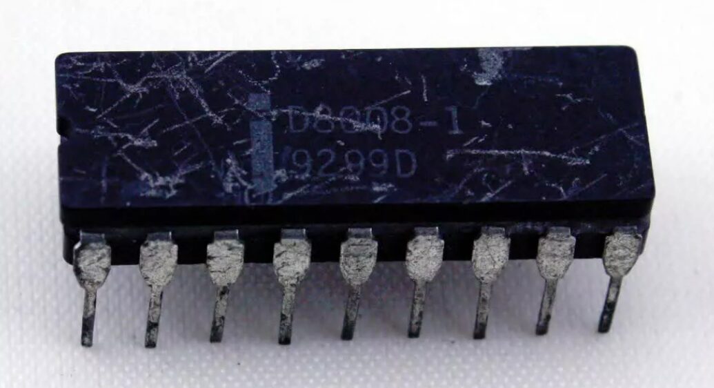
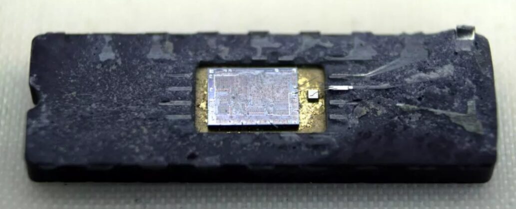
Since I prefer to avoid boiling nitric acid, I took a simpler approach. The 8008 also has a ceramic package (shown above), which I bought on eBay. I used a chisel to tap along the seam of the chip to separate the two layers of ceramic. The image below shows the lower half of the ceramic package, exposing the bare chip. Most of the metal pins have been removed, but their positions in the package are visible. A small square on the right side of the die connects ground (Vcc) to the substrate. A few tiny bonding wires are still visible, connected to the chip.
Once the chip is exposed, it can be photographed using a microscope. Standard microscopes emit light from below, which is not ideal for taking photos. Instead, I used a metallurgical microscope that illuminates the chip from above.
I took 48 photos through the microscope and then used Hugin stitching software to combine them into one high-resolution image. Finally, I adjusted the image contrast to make the chip’s structure clearer. The original image (approximately what you would see through a microscope) is shown below for comparison.
Conclusion
Although the 8008 was not the first microprocessor, nor even the first 8-bit microprocessor, it was indeed revolutionary, sparking the microprocessor revolution and leading to the x86 architecture that dominates personal computing for decades to come.
In later articles, I plan to explain the circuits of the 8008 in detail to give you a glimpse of the roots of today’s computers.