From the perspective of underlying hardware, this article analyzes how the CPU recognizes and reads code. The content is so fascinating that after reading it, I felt that many things I learned suddenly connected together. I wanted to share it with everyone.
Let’s first talk about semiconductors. What is a semiconductor? It is something that is between a conductor and an insulator, such as a diode. Related article: Basic knowledge about diodes.
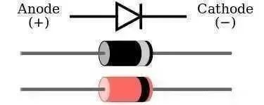
Current can flow from point A to point C, but not the other way around. You can think of it as something that prevents current from flowing backward.
When point C is at 10V and point A is at 0V, the diode can be considered as open.
When point C is at 0V and point A is at 10V, the diode can be considered as a wire, resulting in a continuous flow of current from point A to point C, leading to the final result of A = C = 10V.
Wait, wasn’t it said that C is at 0V and A is at 10V? How did it end up with A = C = 10V? You can think of this as the initial state; once it stabilizes, it will become A = C = 10V.
Sorry to the humanities students, if you don’t understand, just ask your high school physics teacher. If you can’t understand, just remember that in this case, it is equivalent to a wire.
Using this property of semiconductors, we can create some interesting circuits, such as the AND gate.
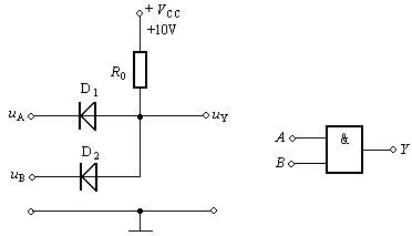
At this time, if either point A or point B is at 0V, then point Y will directly connect to the 0V point, causing point Y to also become 0V. Only when both A and B are at 10V will there be no current flowing between Y and AB, and point Y will also be 10V.
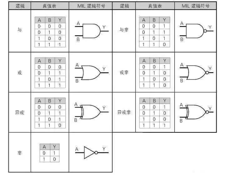
We call this device an AND gate, where a place with voltage is counted as 1, and a place with 0 voltage is counted as 0. As for the specific voltage, it doesn’t matter. This means that both A and B must input 1 simultaneously for output Y to be 1; if either A or B is 0, then output Y is 0.
There are also OR gates, NOT gates, and XOR gates, which are similar. An OR gate outputs 1 if at least one input is 1, and outputs 0 if both inputs are 0.
A NOT gate is also easy to understand: it outputs 0 for input 1 and outputs 1 for input 0.
XOR gates are a bit harder to understand, but it’s not too complicated; it outputs 1 for inputs 01 or 10, and outputs 0 for inputs 00 or 11 (i.e., if both inputs are the same, it outputs 0; if both inputs are different, it outputs 1).
These gates can be made using diodes or transistors; I won’t demonstrate how to do it here, but interested readers can try it themselves. Of course, in reality, they are not made with diodes or transistors because they consume too much power. They are actually made with field-effect transistors (also known as MOSFETs).
Then we can use gate circuits to make a CPU. Of course, making a CPU is still quite difficult; let’s start simple: with an adder. Related article: How does the CPU perform digital addition? An adder, as the name suggests, is a circuit used for addition, and the simplest one is the one below.
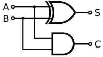
AB can only input 0 or 1, meaning this adder can calculate 0+0, 1+0, or 1+1.
The output S is the result, while C indicates whether a carry has occurred; binary 1+1=10, so at this time, C=1 and S=0.
After spending a lot of effort, isn’t it particularly rewarding to calculate 1+1?
Then let’s further calculate 1+2 (binary 01+10), and we discover a new problem: the second bit needs to handle the possibility of a carry from the first bit, so we need to design a full adder.
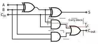
It’s too troublesome to draw every time, so let’s simplify it.
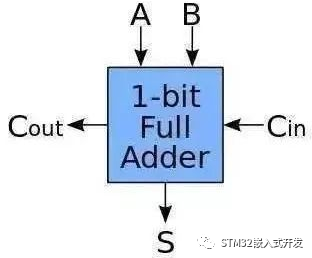
There are 3 inputs and 2 outputs, which are the two numbers to be added and the carry from the previous bit, then the output result and whether there is a carry. Then we can connect this full adder in series:
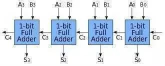
We now have a 4-bit adder that can calculate the addition of 4-bit numbers, which means 15+15, reaching the level of kindergarten middle class. Isn’t that impressive?
After completing the adder, let’s make a multiplier. Of course, multiplying arbitrary decimal numbers is a bit complicated, so let’s start with multiplying by 2.
Multiplying by 2 is quite simple; for a binary number, we just add a 0 at the back. For example:
5=101 (2)
10=1010 (2)
We just need to shift all the inputs forward by one position and add a zero at the lowest position to multiply by 2. I won’t draw the specific logic circuit diagram; you just need to know how it works.
What about multiplying by 3? Simple, shift once (multiply by 2) and then add once. What about multiplying by 5? Shift twice (multiply by 4) and then add once.
So generally, simple CPUs do not have multiplication, and multiplication is implemented through a combination of shifting and addition in software. This is a bit far off; let’s continue with the CPU.
Now, suppose you have an 8-bit adder and a module for shifting by 1 bit. By connecting them, you can calculate (A+B)×2! Exciting, you’re almost at the level of a primary school student.
What if I want to calculate A×2+B? Simple, just change the wiring of the adder module and the shift module so that input A goes through the shift module first, then into the adder.
You mean I have to rewire after changing a program?
What do you think?
In fact, programming is just about plugging wires back and forth. Surprised? Unexpected?
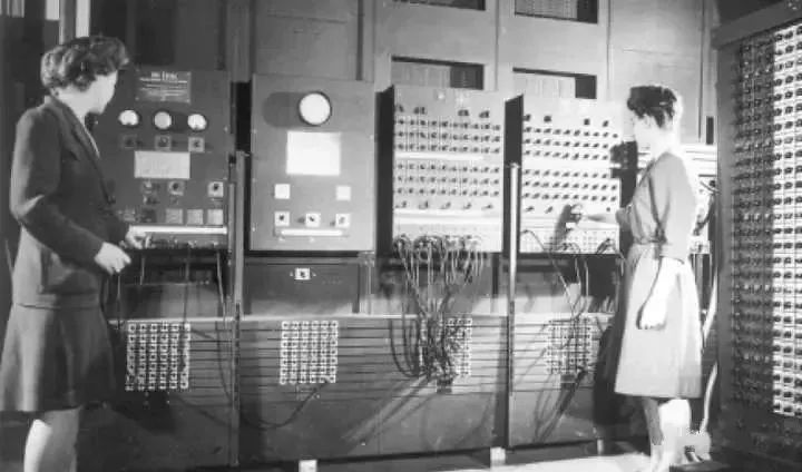
Early computers were programmed this way; it took minutes to compute but took several days to wire. For related articles on wiring programming, you can check out the article: A domestic master manually soldered to create a CPU. Moreover, wiring is a meticulous and patience-requiring task, so back then, all programmers were pretty girls, the kind in uniforms, just like in the photo. Doesn’t that make you feel like you were born in the wrong era?
Wiring is also a tiring job. So we need to improve it, allowing the CPU to add or multiply by 2 according to instructions. Here we introduce two more modules: one called flip-flop, abbreviated as FF, which seems to be called a trigger in Chinese, as shown in the image below.
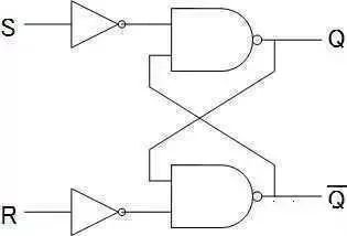
This module is used to store 1-bit data. For example, the RS type FF shown above has R as Reset, inputting 1 clears it. S is Set, inputting 1 saves 1. When both RS are input as 0, it will continuously output the content that was just saved.
We use FF to store intermediate data of calculations (it can also be intermediate states or something else); 1 bit is definitely not enough, but we can parallel them, using 4 or 8 to store 4-bit or 8-bit data. This is what we call a register. The other one is called MUX, which is called a selector in Chinese, as shown in the image below.
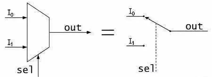
This one is simpler; if sel inputs 0, it outputs the data from i0, whatever i0 is, it outputs it. Similarly, if sel inputs 1, it outputs the data from i1. Of course, selectors can be made long, such as this four-to-one selector; the specific principle is not detailed here, but you can figure it out by looking at the logic diagram, just knowing that this thing exists is enough.
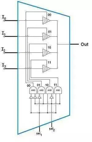
With this, we can design an activation pin for the adder and multiply by 2 module (shift).
This activation pin inputs 1 to activate this module and inputs 0 to deactivate it. This way, we can control whether the data flows into the adder or the shift module.
Thus, we first design 8 input pins for the CPU, 4 for instructions and 4 for data.
We then design 3 instructions:
-
0100, data read into register
-
0001, data adds to register, result saved to register
-
0010, register data shifts left by one bit (multiply by 2)
Why design it this way? As mentioned earlier, we can design an activation pin for each module. We can connect the second, third, and fourth input pins of the instruction to the activation pins of the register, adder, and shift module, respectively.
This way, when we input the instruction 0100, the register input is activated, and other modules are 0 and not activated, so the data is stored in the register. Similarly, if we input the instruction 0001, the adder starts working, and we can perform the addition operation.
This can simply answer the first small question of this article: Why can the CPU understand these binary numbers?
The CPU can understand it because the wires inside the CPU are connected this way. When you input a binary number, it activates certain specified modules inside the CPU and changes the connection methods of these modules, ultimately yielding results.
Some questions that might be asked
Q: The CPU may have thousands of small modules; can a 32-bit/64-bit instruction control that many?
A: In the CPU we are using as an example, there are only 3 modules directly connected. In a real CPU, there will be a decoder that translates the instruction into the required format.
Q: What happens if I input the instruction 0011 into your example CPU?
A: Of course, both the adder and the shift module would be activated simultaneously, leading to unpredictable consequences. Simply put, because you used an unplanned instruction, the consequences are yours to bear. In a real CPU, doing this would likely cause a crash, but there would certainly be various protective designs.
Careful readers might notice a problem: The instruction you designed, [0001, data adds to register, result saved to register], cannot be done in one step, right?
After all, there is still a write-back process. In fact, our simplified CPU executes an instruction in about three steps: read the instruction, execute the instruction, and write to the register.
The classic RISC design divides it into 5 steps: instruction fetch (IF), instruction decode (ID), instruction execution (EX), memory operation (MEM), and write back (WB). Some instructions of the x86 CPU we commonly use may take nearly 20 steps.
You can think of it as a switch; when you press it, the CPU takes one step, and the faster you press, the faster the CPU moves. Oh? You have an idea? Young man, that idea is quite dangerous. Not to mention whether you can press that fast. For modern CPUs, they only go up to about 2GHz, which means you can only press the switch about 20 billion times a second.
Even if you could press that fast, while the speed increases, power consumption would rise significantly, heat would increase, and stability would decrease. There are indeed such practices in the industry, called overclocking, but beginners are not recommended to try it.
How does the CPU know where it is in the process? Didn’t we introduce FF earlier? This can not only be used to store intermediate data but also to store intermediate states, indicating where it is in the process.
The specific design involves FSM (finite-state machine) theory and how to implement it with FF. This is also a very important part and is often tested, but it is not closely related to this topic, so I won’t go into detail here.
Let’s continue with the previous discussion. Now we have 3 instructions. Let’s try to calculate (1+4)×2+3.
0100 0001; register stores 1
0001 0100; register number adds 4
0010 0000; multiply by 2
0001 0011; add three
Awesome! With this computer, we should be able to defeat all kindergarten kids and dominate the middle class! Moreover, we are using 4 bits; if we switch to an 8-bit CPU, we can completely crush lower-grade elementary students!
In fact, controlling the CPU with programs is a quite advanced idea; before this, the CPUs of computers were designed separately.
In 1969, a Japanese company BUSICOM wanted to make a programmable calculator, and the American company responsible for designing the CPU also thought it was quite silly to redesign the CPU every time. So they hit it off and launched a groundbreaking product in 1970, the world’s first microprocessor, the 4004.
This architecture changed the world, and the American company that designed the CPU gradually became an industry giant. Oh, by the way, it’s called Intel, yes, that Intel.
Let’s organize the program we just wrote:
“01000001000101000010000000010011”
Input this into the CPU, and I will prepare to challenge the kindergarten.
What!? By the time we finish inputting, the kids can count with their fingers?
There’s no way; machine language is just that inhumane. Oh, I forgot to mention that this language made up solely of 0s and 1s is called machine language (machine code), the only language that the CPU can understand. However, if you let people read machine language, they would instantly turn into a dictionary; no one can stand that.
So let’s improve it a bit. However, it was only about 30 years ago that directly inputting 0s and 1s was quite common.
So, we rewrite our machine language program:
MOV 1; register stores 1
ADD 4; register number adds 4
SHL 0; multiply by 2 (since our designed multiplier can only multiply by 2 for now, this 0 is a placeholder)
ADD 3; add three
Isn’t it easier to read? This is called assembly language.
The advantage of assembly language is that it corresponds one-to-one with machine language.
This means that the assembly we write can be perfectly rewritten into machine language to directly command the CPU for low-level development; we can also dump data from memory in the form of assembly language for debugging.
Assembly language greatly enhances the readability and development efficiency of machine language, but it is still too obscure for humans. Therefore, we invented high-level languages that express data structures and algorithms in a syntax closer to human language.
For example, many languages can write it like this:
a=(1+4)*2+3;
Of course, the computer doesn’t recognize this; we need to translate it into a form the computer understands, and this process is called compilation. The tool used for this is called a compiler.
The specifics of how to convert high-level languages into assembly language/machine language could fill a book, so I’ll just give a simple example.
We convert:
(1+4)*2+3
into:
1,4,+,2,*,3,+
This notation is called postfix notation, also known as Reverse Polish Notation (RPN). In contrast, the notation we usually use is called infix notation, where the operator is placed between the operands, such as 1+4. Postfix notation is written as 1,4,+.
The benefit of converting to this notation is that it eliminates the influence of precedence (multiplication before addition) and parentheses; you can just calculate directly.
The specifics of how to convert can be found in a book on compiler principles; I won’t elaborate here.
Once converted to this form, we can turn it into assembly language.
Starting from the beginning, the first is 1, a number, so we store it in the register:
MOV 1
Next is 4, +, so we add:
ADD 4
Next is 2, *, so we multiply (since our designed multiplier can only multiply by 2 for now, this 0 is a placeholder):
SHL 0
Finally, 3, +, so we add:
ADD 3
Finally, we organize the translated assembly:
MOV 1
ADD 4
SHL 0
ADD 3
Then simply convert it into machine language, and we can run it on our designed simple CPU.
At this point, we should have clarified this question: How is the C language translated into binary, and how does the computer run this binary?
However, the questioner also mentioned the relationship between stacks and hardware, so let’s elaborate a bit more.
In fact, a stack is a data structure that is not related to the CPU. However, the stack data structure is so commonly used that the CPU is optimized for it. To enable our CPU to use stacks, we add a few components.
First, we add a set of registers. Now we have two sets of registers, which we call A and B.
Second, we add two instructions, RDA/RDB and WRA/WRB, which respectively read data from a specified memory address into registers A/B and write the contents of registers A/B to the specified address.
By the way, let’s talk about memory. Memory has an address bus and a data bus. For example, if you want to store the number 1100 at address 0011, you connect 1100 to the data bus and 0011 to the address bus, prepare everything, and then press the switch (yes, that switch we mentioned earlier), and it’s stored.
What is DDR memory? It means that when you press this switch, you store one number, and before you lift it, you update the address and data, and then release it, and another number goes in. This means that normal memory stores one data per press, while DDR memory stores two data per press, hence the name Double Data Rate (DDR).
After adding these commands, we find that if we stick to the original design where each instruction pin controls one module, there aren’t enough pins. So we need to add a decoder.
We choose to use the second bit as the pin to select the register. If it is 0, the third and fourth bits can normally activate the shift and adder; if it is 1, only the register is activated without activating the shift and adder, and then the fourth bit decides whether it is register A or B.
Thus it becomes:
-
0100, data read into register A
-
0101, data read into register B (we define the assembly instruction as MOVB)
-
0001, data adds to register A, result saved to register A
-
0011, data adds to register B, result saved to register B (we define the assembly instruction as ADDB)
-
0010, data in register A shifts left by one bit (multiply by 2)
Finally, we can use the first bit to control whether to perform memory operations. If the first bit is 1, then it also does not activate the shift and adder modules, and the third pin controls whether to read or write. This gives us:
-
1100, read the address data from register B into register A (we define the assembly instruction as RD)
-
1110, write the data from register A to the specified address in register B (we define the assembly instruction as WR)
After adding a decoder, the activation condition for the adder changes from p4 to (NOT (p1 OR p2)) AND p4.
The input for the adder is determined by the third pin; 0 is register A, and 1 is register B. This is the simple instruction decoding.
Of course, we could choose not to maintain backward compatibility and design a whole new set of instructions. However, in the real world, this could lead to major chaos, so you can imagine how heavy the historical burden on the x86 architecture is.
At this point, if we want to use stacks, we first initialize the stack address:
0101 1000; MOVB 16; define the base address of the stack as 1000
Then, to push onto the stack, for example, to push the numbers 3 and 4:
1111 0011; WR 03; write 3 to memory at address 1000
0011 0001; ADDB 01; increment stack address by 1
1111 0100; WR 04; write 4 to memory at address 1001
0011 0001; ADDB 01; increment stack address by 1
This way, we have saved 3 and 4 onto the stack.
To pop from the stack, it’s the reverse:
0011 1111; ADDB -1; decrement stack address by 1
1101 0000; RD 00; read the content into register A, 00 is a placeholder
0011 1111; ADDB -1; decrement stack address by 1
1101 0000; RD 00; read the content into register A, 00 is a placeholder
This way, we get the values 4 and 3 in sequence.
Thus, pushing and popping are essentially writing data to specified memory locations; the CPU itself doesn’t know what you are doing. Related article: A classic explanation of the stack in C language.
Of course, we can also let the CPU know.
Next, let’s improve it a bit by adding a register SP to the CPU and defining two instructions: PUSH and POP. The actions are to write data to the address of SP and then SP=SP+1 for PUSH, and the reverse for POP.
What’s the benefit of this? The advantage is that instructions like PUSH/POP consume very little and are very fast. Since the stack data structure is used very frequently in various programs, designing it as a dedicated instruction can greatly enhance efficiency.
Of course, the premise is that the compiler knows this instruction and has optimized it, so the same program (written in C language) can produce different outputs with different compilation parameters (enabling/disabling certain features), resulting in different efficiencies on different hardware.
For example, in ancient times, MMX; today, SSE4.2, AVX-512, powerful, right? It’s very powerful, but whether the programs you usually use support it is another matter. How to support it? Recompile.
This is where the advantage of open-source shows; recompiling is very convenient. For closed-source, you have to rely on the author’s kindness.
For most people, computers are black boxes, and it’s hard for us to understand how they work. This question is difficult to explain clearly in just a few sentences because it is a chain of interconnected concepts, each of which is very abstract, and each layer is worth two credits, with no limit on how much it can be expanded.
This leads to the fact that even those who have studied computer science may not have a clear and definite understanding of it. I hope to explain this matter from beginning to end in as few words and as simply as possible, hoping to clarify some doubts for everyone. For more on the combination of software and hardware, I also recommend this article: How does code control hardware?
(The End)
More exciting content:
Yan Shi | Thoughts and Suggestions on the “Predicament” of Young Teachers in Higher Education
【Directory】 “Computer Education” 2022, Issue 8
【Directory】 “Computer Education” 2022, Issue 7
【Directory】 “Computer Education” 2022, Issue 6
【Directory】 “Computer Education” 2022, Issue 5
【Editorial Board Message】 Professor Li Xiaoming from Peking University: Thoughts from the “Year of Classroom Teaching Improvement”…
Professor Chen Daoxu from Nanjing University: Teaching students to ask questions and teaching students to answer questions, which is more important?
【Yan Shi Series】: Trends in Computer Science Development and Their Impact on Computer Education
Professor Li Xiaoming from Peking University: From Fun Math to Fun Algorithms to Fun Programming — A Path for Non-Majors to Experience Computational Thinking?
Several Reflections on Building a First-Class Computer Science Discipline
New Engineering and Big Data Major Construction
Other countries’ stones can be used to attack jade — A Compilation of Research Articles on Computer Education at Home and Abroad