🔍See the article below for program acquisition methods
🔍The project includes complete programs, comments, references, and operation videos
⚡️Algorithm Simulation Effect Preview
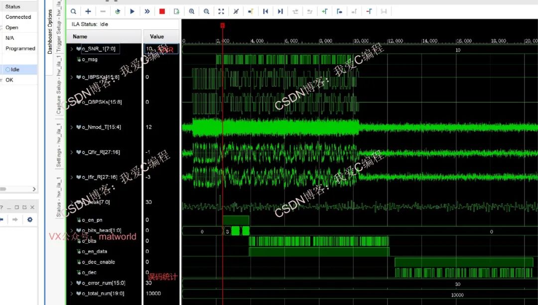
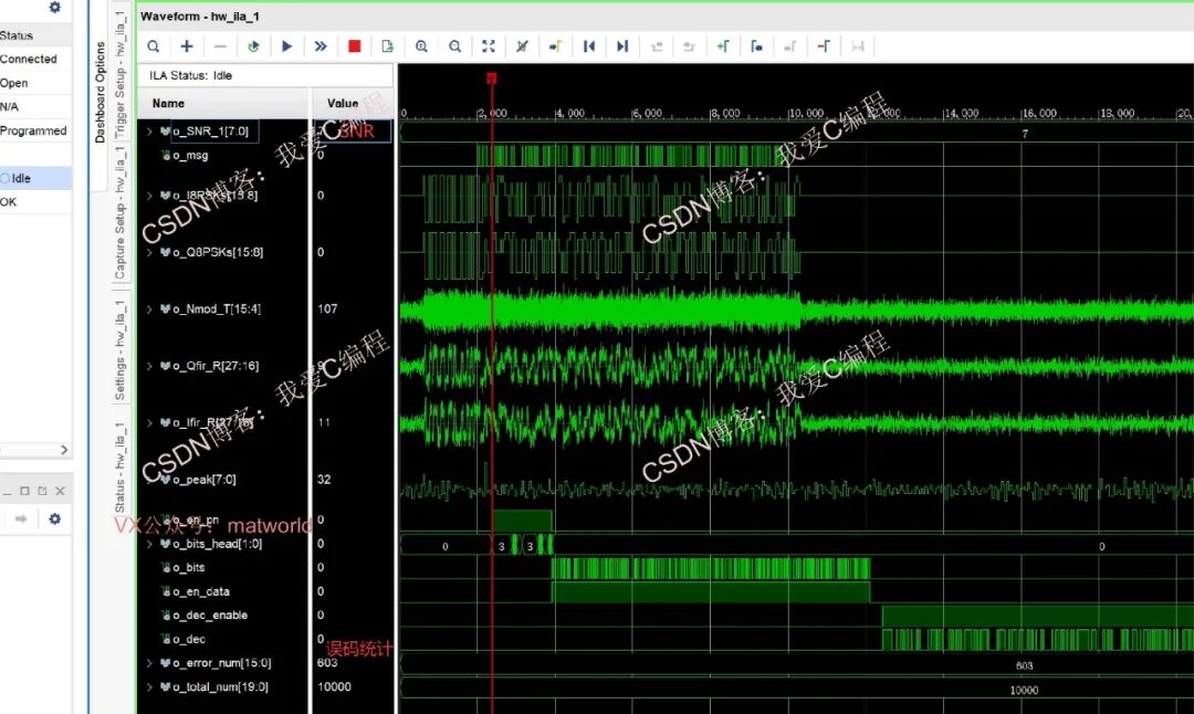
The simulation test results using Vivado 2022.2 are as follows (217 convolution encoding and decoding Verilog development, without using IP cores):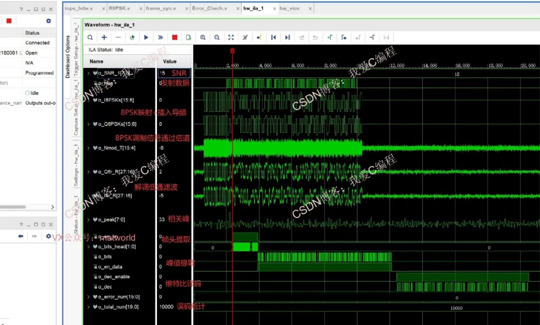
🚀System Overview
1. 8PSK
8PSK modulation is a type of phase modulation where information is transmitted by changing the phase of the carrier wave. In 8PSK, there are 8 possible phase states within one symbol period, corresponding to 3 bits of information. Therefore, 8PSK modulation can be seen as a mapping of 3 bits to one symbol. Specifically, assuming the input bit sequence is b2b1b0, the corresponding 8PSK symbol can be represented as:
S(t)=Acos(2πfct+θk) (1)
where A is the amplitude of the carrier, fc is the frequency of the carrier, and θk is the phase of the k-th symbol, k=0,1,…,7. The value of θk is determined by the input bit sequence b2b1b0, with the specific mapping relationship shown in Table 1.
2. Frame Synchronization
In digital communication, information is typically organized and transmitted in frames. The purpose of frame synchronization is to determine the starting position of each frame so that the receiver can correctly demodulate the data within each frame.
Assuming the transmitted frame structure is: frame synchronization code + information code element sequence. The frame synchronization code is a code sequence with a specific pattern used for the receiver to identify the start of the frame.
The process of frame synchronization involves searching for positions in the received sequence that match the frame synchronization code. Once a matching position is found, the starting position of the frame is determined, and subsequent code elements can be correctly divided and processed according to the frame structure.
3. Convolutional Encoding and Viterbi Decoding
Convolutional encoding is a type of forward error correction coding, particularly suitable for wireless communication and other applications with poor channel conditions. It mainly maps the information sequence into a codeword sequence with higher redundancy using a convolution operator. A typical convolutional encoder consists of two shift registers and an adder, following a specific generating polynomial for encoding.
Let the information sequence be u(n), and the two generating polynomials of the convolutional encoder be G1(D) and G2(D), then the encoding output v(n) can be expressed as:
v(n)=u(n)G1(D)+u(n−1)G2(D)+…
Here, D is the delay operator, and the actual expression depends on the specific choice of the order and coefficients of the generating polynomial.
Viterbi decoding is a dynamic programming algorithm used for maximum likelihood sequence estimation, widely applied in the decoding process of convolutional encoding and other sequence encoding. In convolutional encoding, the Viterbi decoder constructs a tree structure called a “state transition graph” or “trellis” to find the most likely path of the original information sequence.
In the Viterbi decoding algorithm, each step requires calculating branch metrics, path metrics, and updating surviving paths, while also needing to know the state transition grid, timing control, and other information, as shown in the diagram:
Assuming the Viterbi decoder is facing a received codeword sequence y(n) with noise, its goal is to minimize the Hamming distance or maximize likelihood. The core of the Viterbi algorithm is to maintain the state probabilities at each step and the accumulated cost of the best path from the initial state to the current state.
State transition equation: For each time n and each state Sj, the best path accumulated cost C(n,Sk) for the next state Sk can be recursively expressed as the accumulated cost of all previous states Sj plus the corresponding path probability gain:
C(n,Sk)=Sj∈prev(Sk)min[C(n−1,Sj)+P(y(n)∣Sk)]
where prev(Sk) represents the set of predecessor states of state Sk, and P(y(n)∣Sk) is the probability of observing y(n) given the current state Sk.
Termination state decision: At the end of decoding, the path corresponding to the termination state with the minimum accumulated cost is selected as the optimal solution, and backtracking this path yields the optimal decoding result.
✨Some Core Code
..`timescale 1ns / 1ps//////////////////////////////////////////////////////////////////////////////////// Company: // Engineer: // // Create Date: 2025/08/16 14:59:12// Design Name: // Module Name: tops_hdw// Project Name: // Target Devices: // Tool Versions: // Description: // // Dependencies: // // Revision:// Revision 0.01 - File Created// Additional Comments:// //////////////////////////////////////////////////////////////////////////////////

module tops_hdw(
input i_clk,input i_rst,output reg [3:0] led);


// Generate simulated test data
wire signed[1:0]o_en;
wire            o_msg;
wire            dat_clk;
wire            dat_2clk;
signal signal_u(.i_clk (i_clk),.i_rst (~i_rst),.o_en(o_en),.o_bits(o_msg),.dat_clk(dat_clk),.dat_2clk(dat_2clk));


// Set SNR
wire signed[7:0]o_SNR;
vio_0 your_instance_name (  .clk(i_clk),                // input wire clk  .probe_out0(o_SNR)  // output wire [7 : 0] probe_out0);
wire [1:0]o_enc;
wire      o_encs;
wire[2:0]o_ISET;
wire signed[15:0]o_I8PSK;
wire signed[15:0]o_Q8PSK;
wire signed[15:0]o_I8PSKs;
wire signed[15:0]o_Q8PSKs;
wire signed[31:0]o_mod_T;
wire signed[15:0]o_Nmod_T;
wire signed[31:0]o_modc_R;
wire signed[31:0]o_mods_R;
wire signed[31:0]o_Ifir_R;
wire signed[31:0]o_Qfir_R;
wire  [2:0]o_wbits;
wire       o_bits;
wire [1:0]o_bits_head;
wire [7:0]o_peak;
wire  o_en_data;
wire  o_en_pn;
wire  o_frame_start;
wire o_dec_enable;
wire o_dec;
wire signed[31:0]o_error_num;
wire signed[31:0]o_total_num;
TOPS_8PSK TOPS_8PSK_u(.i_clk        (i_clk),.i_clkdx      (dat_clk),.i_clkd2x     (dat_2clk),.i_rst        (~i_rst),.i_SNR        (o_SNR),.i_en         (o_en),.i_dat        (o_msg),.o_enc        (o_enc),.o_encs       (o_encs),.o_ISET       (o_ISET),.o_I8PSK      (o_I8PSK),.o_Q8PSK      (o_Q8PSK),.o_I8PSKs     (o_I8PSKs),.o_Q8PSKs     (o_Q8PSKs),.o_mod_T      (o_mod_T),.o_Nmod_T     (o_Nmod_T),
.o_modc_R     (o_modc_R),.o_mods_R     (o_mods_R),.o_Ifir_R     (o_Ifir_R),.o_Qfir_R     (o_Qfir_R),.o_wbits      (o_wbits),.o_bits       (o_bits),.o_bits_head  (o_bits_head),.o_peak       (o_peak),.o_en_data    (o_en_data),.o_en_pn      (o_en_pn),.o_frame_start(o_frame_start),.o_dec_enable (o_dec_enable),.o_dec        (o_dec),.o_error_num  (o_error_num),.o_total_num  (o_total_num));

// ILA in-chip testing analysis module 140
// ILA in-chip testing analysis module 140
ila_0 ila_u ( .clk(i_clk), // input wire clk .probe0({ o_msg,o_SNR,o_I8PSKs[15:8],o_Q8PSKs[15:8],//20 o_Nmod_T[15:4],o_Ifir_R[27:16],o_Qfir_R[27:16],o_wbits,//40 o_error_num[15:0],o_total_num[19:0],//40 //28 o_en_pn, o_en_data, o_peak,//8 o_dec_enable,o_dec, o_bits, o_bits_head }) ); endmodule0sj2_087m🌐How to Obtain the Complete Project
Method 1: Copy the link to the browser
https://mbd.pub/o/bread/YZWWl5pvZA==
Method 2: Open the store and search:
http://www.store718.com/List.asp?ID=4742
Method 3: Click 【Read Full Article】 in the lower left corner of the article

Method 4: If the above links are invalid, for program debugging bugs or project collaboration, you can contact via WeChat or QQ.