-
Vivado (Vitis) Version: 2020.2
-
FPGA Development Board: Microphase Z7-Lite 7020 Development Board
FPGA Design Debugging Process
FPGA development is an iterative process, and the general FPGA design process typically includes the following steps:
-
Hardware architecture and algorithm verification: what modules are needed to implement the required functionality, how modules communicate and connect with each other; whether the hardware algorithm is feasible and stable (for example, for image processing algorithms, MATLAB can generally be used for algorithm verification);
-
RTL code writing;
-
Hardware debugging and verification: this process generally consumes a lot of time, and without certain experience and skills, it can significantly extend the development time or even lead to development failure;
Debugging, which is the process of identifying and fixing issues, is often the most complex and frustrating part of design for those with development experience. For a large and complex FPGA project, the probability of encountering issues is very high. Without a clear debugging mindset, the debugging process can feel like aimlessly flailing around. The general debugging approach in FPGA design is as follows:
First, check for hardware issues: when a problem arises, first suspect and eliminate hardware issues. Check if the power supply and connections of the development board are normal, whether any electronic components have been burned out, or if there are any cold solder joints. After confirming that the development board and power supply are functioning properly, test the problematic core components using example routines or existing programs or projects. For example, when reading and writing DDR, if there is no response from the DDR, you can search online for example routines or use the official example routines provided by the development board to test DDR read/write operations, confirming that DDR is functioning correctly; when reading and writing to an SD card, you can try using a different SD card or switch the SD card to another device to ensure it is not damaged. In practical engineering applications, it is necessary to flexibly choose testing and troubleshooting solutions, but the ultimate goal is generally the same.
Next, check global signals: after confirming that there are no hardware connection issues, check for possible problems with global signals. Global signals generally refer to signals that connect all internal modules, such as i_sys_clk and i_sys_rst_n. It is necessary to ensure these signals are functioning correctly before proceeding with RTL checks.
Finally, check the RTL code: after ensuring that there are no issues with hardware and global signals, begin checking the RTL code. There is also a certain order to follow when checking RTL code, which can generally refer to the following sequence:
-
Check the handshake mechanism between master and slave devices (modules), or check whether the master and slave devices are connected correctly. Many times, you can refer to the device’s official datasheet to verify whether the initialization commands between the master and slave modules are written correctly.
-
Check whether state transitions are normal: state machines are often used for RTL programming during initialization.
-
Check whether the read/write data is normal: you can design some “dummy data,” such as predetermined patterned data, to check if these data are correctly located in the addresses of the slave device.
-
Check whether the trigger signal for executing operations is functioning properly: verify whether the trigger signals are working correctly.
In summary, RTL debugging is the most tedious part; often it requires “peeling the onion” and “tracing back to the source” to find the root cause of the problem. However, the author believes that this is precisely a necessary skill and mindset that reflects the hard skills of an FPGA engineer.
Using Vivado ILA IP
ILA, or Integrated Logic Analyzer, is an integrated logic analyzer designed within Xilinx FPGA chips. It can replace traditional external logic analyzers to a certain extent. ILA is usually used in conjunction with VIO (Virtual Input/Output), which can not only monitor internal logic signals and port signals in real-time but also simulate input signals to drive internal ports. ILA monitors internal signals and outputs them to a PC, while VIO receives real-time commands from the PC to provide input signals to internal ports.
There are various methods for ILA debugging; it can be added directly in the code using primitives, added in the schematic through debugging, or added in the netlist.
Here, let’s create an example project using a breathing light module as the top-level code:
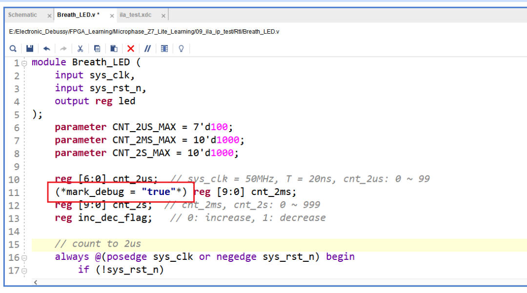
module Breath_LED ( input sys_clk, input sys_rst_n, output reg led); parameter CNT_2US_MAX = 7'd100; parameter CNT_2MS_MAX = 10'd1000; parameter CNT_2S_MAX = 10'd1000; reg [6:0] cnt_2us; // sys_clk = 50MHz, T = 20ns, cnt_2us: 0 ~ 99 reg [9:0] cnt_2ms; reg [9:0] cnt_2s; // cnt_2ms, cnt_2s: 0 ~ 999 reg inc_dec_flag; // 0: increase, 1: decrease // count to 2us always @(posedge sys_clk or negedge sys_rst_n) begin if (!sys_rst_n) cnt_2us <= 7'd0; else if (cnt_2us == (CNT_2US_MAX - 7'd1)) cnt_2us <= 7'd0; else cnt_2us <= cnt_2us + 7'd1; end // count to 2ms by cnt_2us always @(posedge sys_clk or negedge sys_rst_n) begin if (!sys_rst_n) cnt_2ms <= 10'd0; else if ((cnt_2us == (CNT_2US_MAX - 7'd1)) && (cnt_2ms == (CNT_2MS_MAX - 10'd1))) cnt_2ms <= 10'd0; else if (cnt_2us == (CNT_2US_MAX - 7'd1)) cnt_2ms <= cnt_2ms + 10'd1; end // count to 2s by cnt_2ms always @(posedge sys_clk or negedge sys_rst_n) begin if (!sys_rst_n) cnt_2s <= 10'd0; else if ((cnt_2us == (CNT_2US_MAX - 7'd1)) && (cnt_2ms == (CNT_2MS_MAX - 10'd1)) && (cnt_2s == (CNT_2S_MAX - 10'd1))) cnt_2s <= 10'd0; else if ((cnt_2us == (CNT_2US_MAX - 7'd1)) && (cnt_2ms == (CNT_2MS_MAX - 10'd1))) cnt_2s <= cnt_2s + 10'd1; end // inc_dec_flag always @(posedge sys_clk or negedge sys_rst_n) begin if (!sys_rst_n) inc_dec_flag <= 1'b0; else if ((cnt_2us == (CNT_2US_MAX - 7'd1)) && (cnt_2ms == (CNT_2MS_MAX - 10'd1)) && (cnt_2s == (CNT_2S_MAX - 10'd1))) inc_dec_flag <= ~inc_dec_flag; else inc_dec_flag <= inc_dec_flag; end // led PWM configuration always @(posedge sys_clk or negedge sys_rst_n) begin if (!sys_rst_n) led <= 1'b0; else if ((inc_dec_flag == 1'b0) && (cnt_2ms <= cnt_2s)) // increase led <= 1'b1; else if ((inc_dec_flag == 1'b1) && (cnt_2ms >= cnt_2s)) // decrease led <= 1'b1; else led <= 1'b0; endendmoduleIP Core Configuration
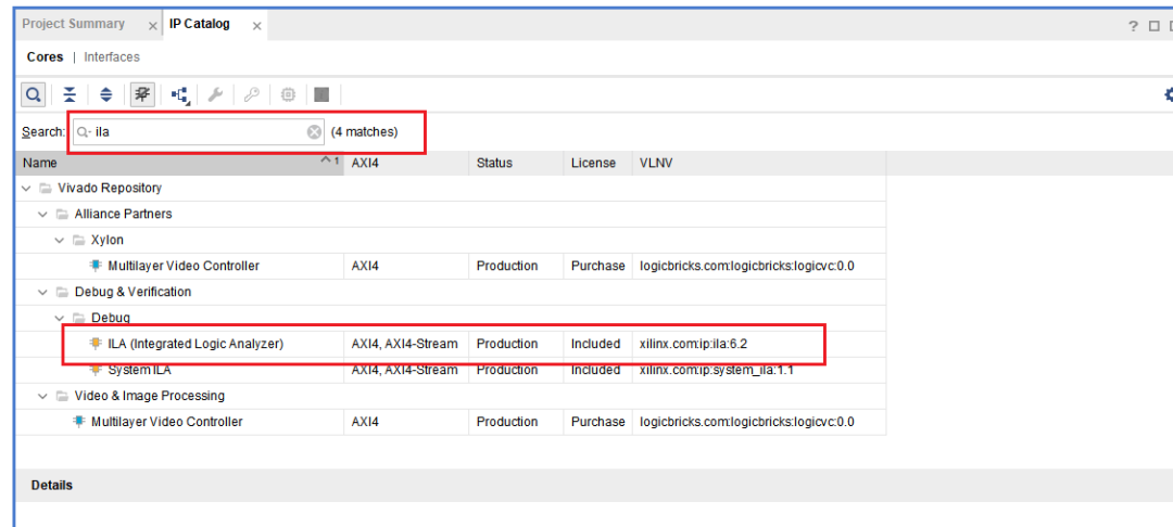
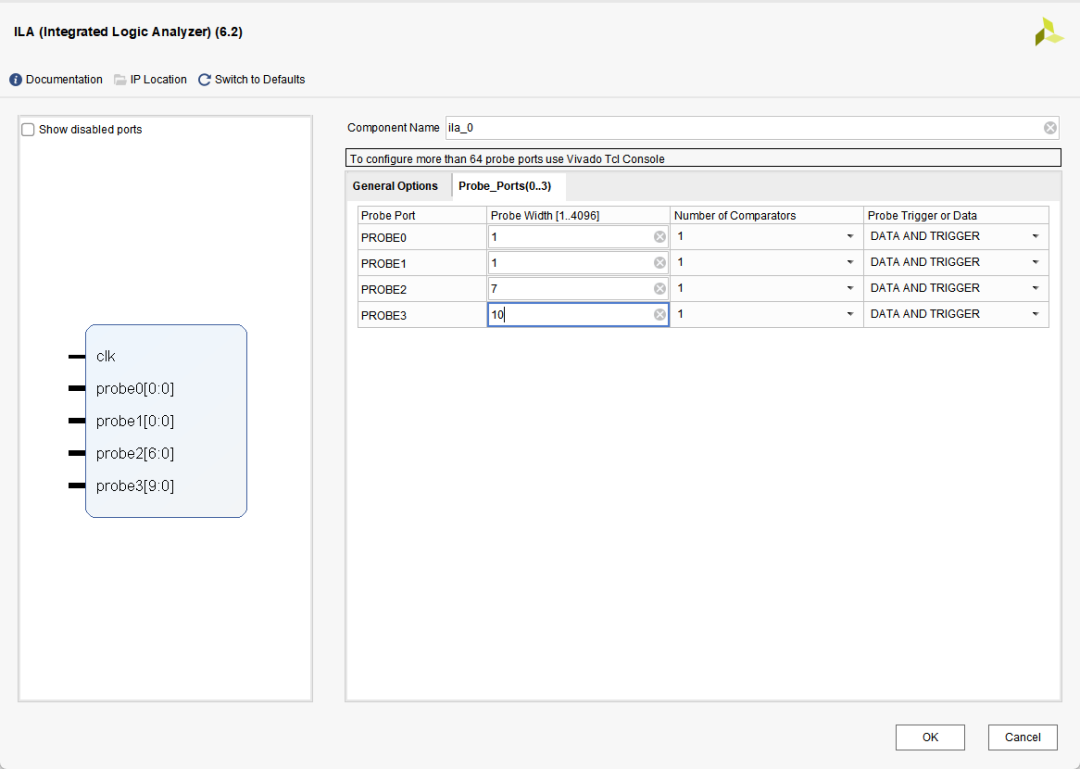
Search for ILA in the IP Catalog to find the ILA IP core, double click it to open the configuration interface.
Set the component name, the number of probes (the number of signals to be measured), and the sampling depth. The clk signal is generally the system clock signal; the ILA IP will sample the corresponding signal data on each rising edge (or falling edge, which needs to be considered) of clk until the number of sampled signals reaches the sampling depth.
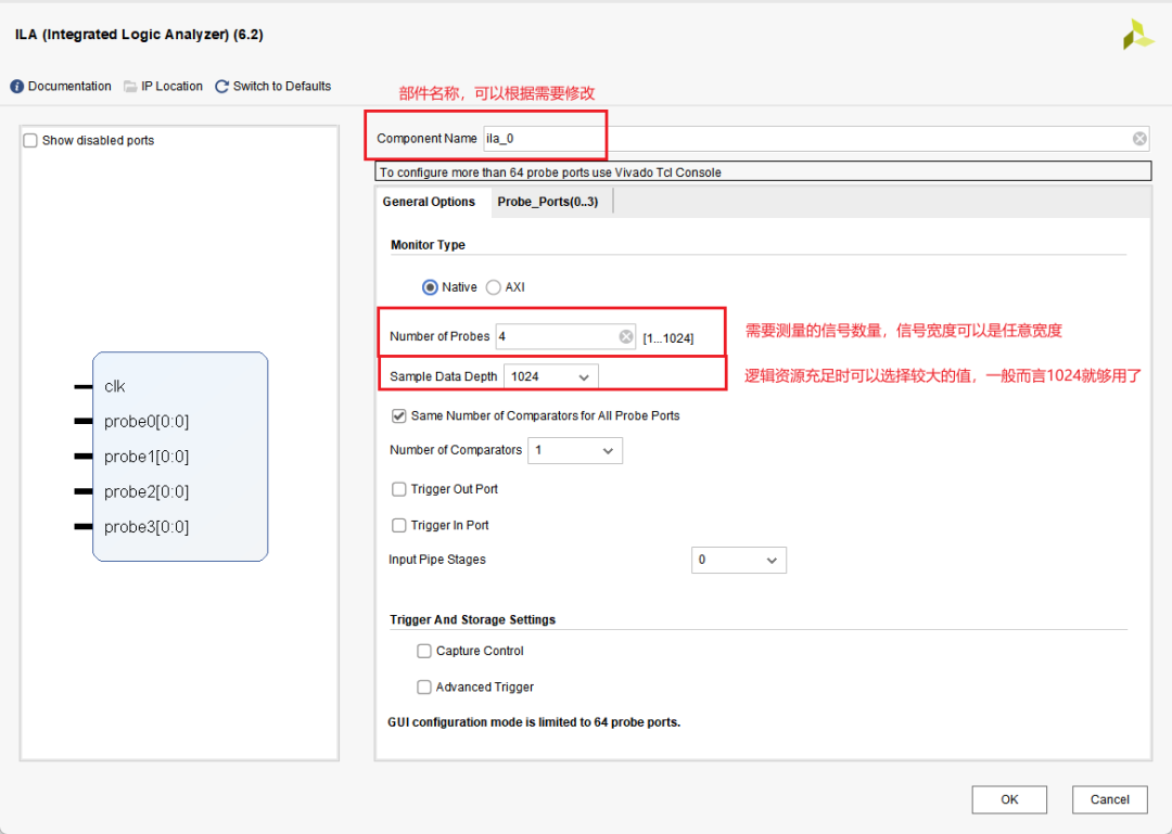
Assuming there is an issue with the code, we need to monitor the signals sys_clk, led, sys_rst_n, cnt_2us, and cnt_2ms. The widths of these signals are 1, 1, 7, and 10 respectively.
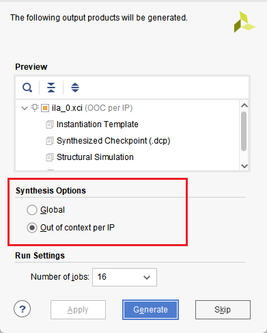
After completing the settings, click OK to see the following interface. If the synthesis option is set to Global, the code will synthesize the ILA every time; if Out of Context per IP (OOC mode) is selected, the code will only synthesize the ILA when the settings change. Generally, the latter is chosen to speed up synthesis.
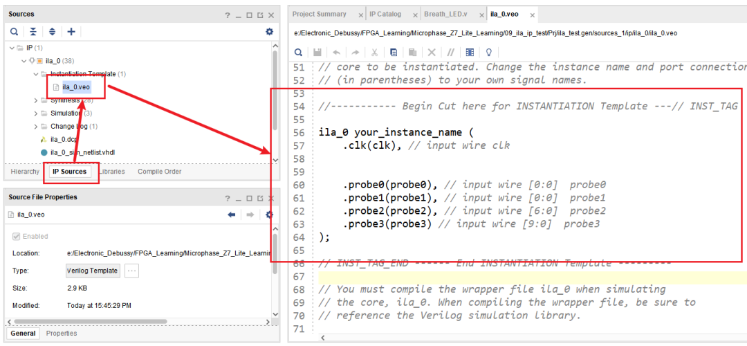
IP Instantiation
First, find the instantiation template in the ila_0.veo file. Copy it to the module needed in the project. In this example, copy it to the top-level file Breath_LED.v. (All IP core instantiations can use this method to obtain instantiation templates)
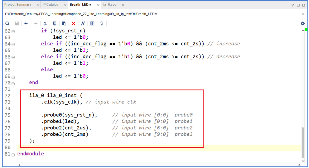
Instantiate and connect the corresponding signals:
Add a constraint file, generate a bitstream file, and program it into the development board.
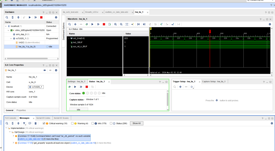
Waveform Analysis
After programming is complete, you can see that the LED on the board has started to breathe. At this point, Vivado will automatically pop up the ILA waveform debugging interface:
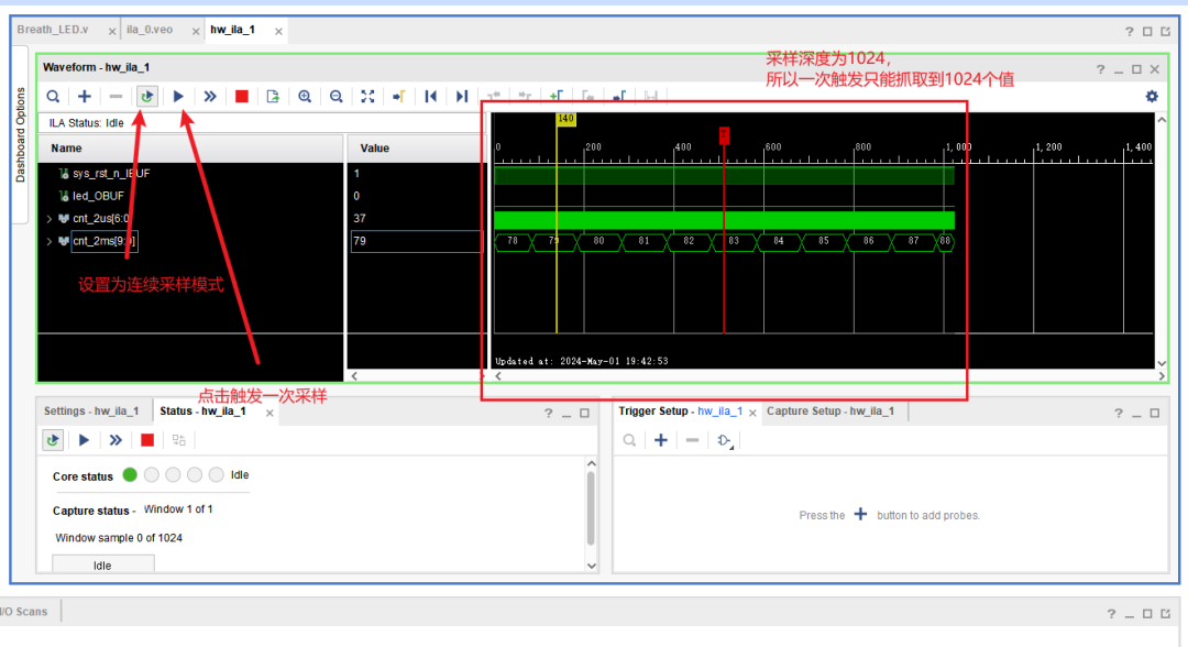
By sampling, you can observe the waveform. In actual development, it is very likely to encounter situations where the values of interest do not change during a single sampling. In such cases, continuous sampling or multiple samples are generally needed, as a single sampling trigger may occur during the FPGA’s bank precharge period or during the initialization of external devices. Sampling multiple times can help identify patterns even if there are design bugs.
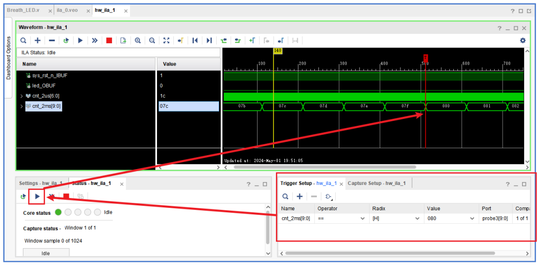
Manual sampling can only display part of the waveform, and the displayed time is very short. However, often the signals we care about appear for a very short time, and we cannot guarantee that every trigger will capture the needed signal or value. At this point, we can set trigger conditions in the lower right window. After clicking single sample, the ILA will attempt to help us capture the specific signal state. If it doesn’t capture, the capture process will not end.
So, how should we add trigger signals when facing an actual complex project filled with bugs? We should start from the output to check if there are issues with the module’s output. If there are no issues, we then find the higher-level output signal to see if there is a problem with the generation mechanism. If there are issues with the output trigger signal or counter, we will check how that trigger signal or counter is generated to see if there are bugs… and so on, tracing back until we find the bug and ensure functionality.
After adding the ILA IP and marking debug signals, the corresponding content will be automatically generated in the constraint file. Do not delete these debug-related constraints, as it may lead to errors.
Debug Signals in the Schematic
After testing, the author found that this method is not very effective and may encounter errors in Vivado or issues finding the debug ltx file. This method is not recommended.
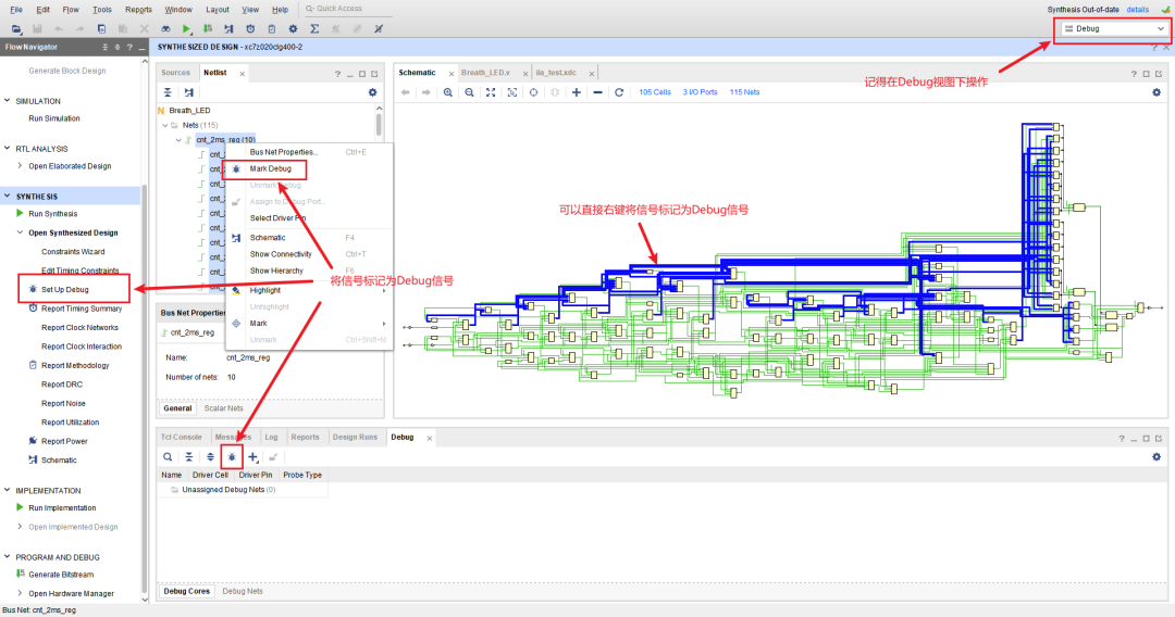
Debugging signals via the schematic essentially has the same effect as adding ILA IP; the only difference is in how the signals are debugged. Adding debug signals in the schematic does not require creating and instantiating IP cores; after synthesizing the code, simply open the schematic window and find the debug view.
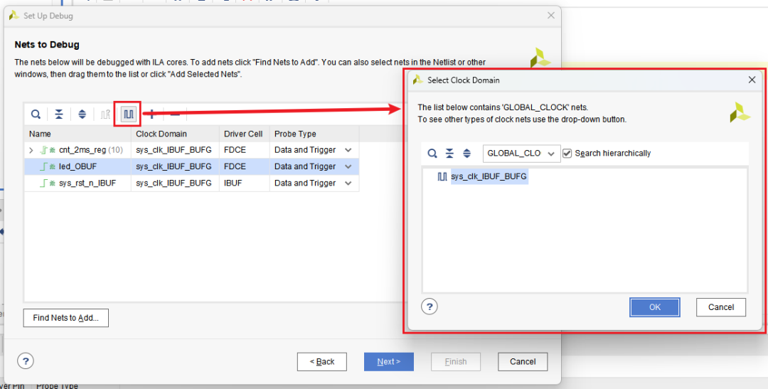
You can also add debug signals in the Set Up Debug wizard.
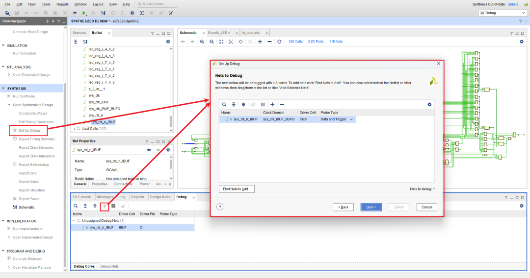
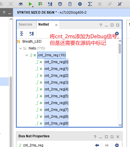
You can directly mark signals as debug signals in the netlist. However, it is important to note: for input/output signals, do not mark the original signals as debug signals; you must mark the corresponding IBUF or OBUF as debug signals, otherwise Vivado may throw errors.
If the signal to be added does not have a corresponding IBUF or OBUF, such as needing to mark an internal counter as a debug signal, you need to mark the signal in the netlist and also in the source code definition; otherwise, Vivado may optimize (eliminate) that signal during synthesis since it does not pass through IBUF and OBUF, even if it is an internal signal. After marking, Vivado will not optimize that signal during synthesis but will retain it.
In the Set Up Debug wizard, set the clock domain, which is the clock that triggers ILA sampling.
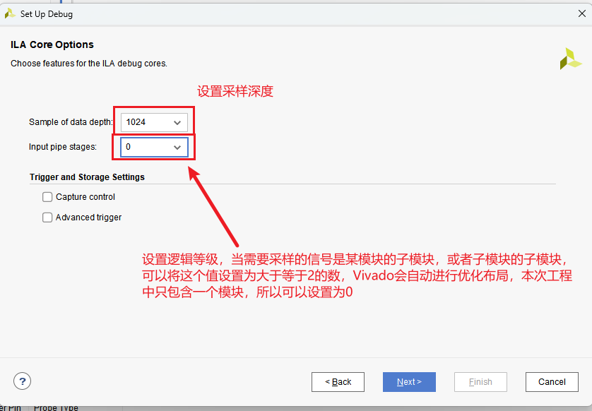
Click Next to set the sampling depth and logic levels.
The subsequent operations are no different from debugging with IP cores.