 Introduction: Previously, I introduced the manufacturing and packaging of chips. In this article, we will look at chip design.█ Design Concepts of ChipsAs we all know, chips have extremely complex structures.Taking NVIDIA’s B200 chip as an example, it contains 208 billion transistors in an area the size of a palm. The layout inside is akin to a labyrinth of another dimension.
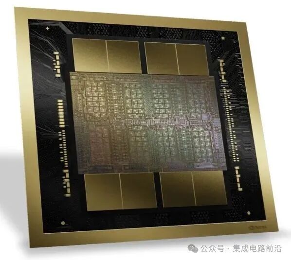 NVIDIA B200 ChipThis complex architecture presents significant challenges in both manufacturing and design.In the early days of integrated circuits, the number of transistors was not high, and the structure was not complex.Thus, design engineers would directly draw the physical layout of the circuit on paper and send the layout to the manufacturing plant for production.
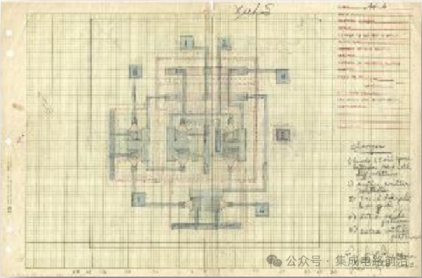 Early Hand-Drawn Logic Circuit Diagrams (from Fairchild Semiconductor)The hand-drawn layouts were very detailed, specifying the physical levels of transistors, including layout and wiring.
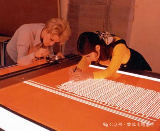 Early Handcrafted Masks (1970)As integrated circuits became increasingly complex, they continued to use this method, first drawing the lower-level details and then “stitching” them together to form a complete integrated circuit.This design concept is calledBottom-Up Design.
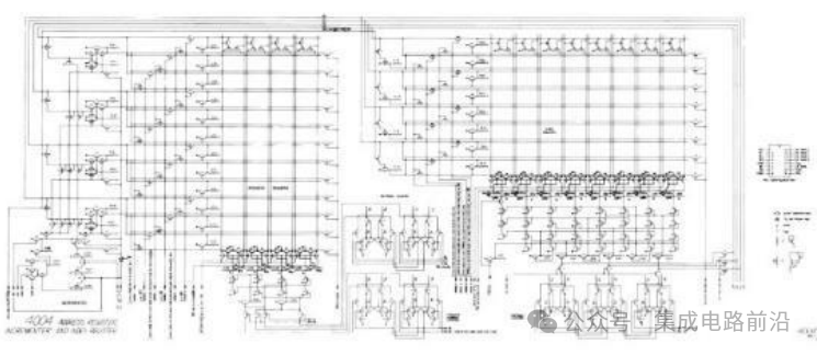 Design Diagram of Intel 4004 Chip (1971)It should be noted that from a design perspective, a chip is divided into different levels.From top to bottom, they are: system level, RTL level, gate level, transistor level, layout and routing level, and mask level.
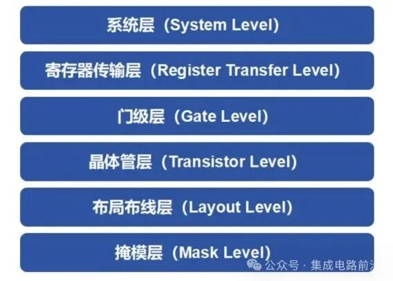 The system level is the highest level, providing an overall design of the chip from a macro perspective.The RTL level is the Register Transfer Level. The “gates” in the gate level are logic gates, which are built from transistors.The mask, as previously introduced in wafer manufacturing, is the photomask, which is the final product of chip design and the lowest level that can describe the chip in detail. The mask layer is the lowest layer.Bottom-Up Design is suitable for early integrated circuits and traditional PCB circuits.By the 1970s and 1980s, integrated circuits evolved into large-scale and very large-scale integrated circuits, with transistor counts exceeding 10,000.At this point, using theBottom-Upapproach became inappropriate. Thus, theTop-Downdesign concept began to emerge.
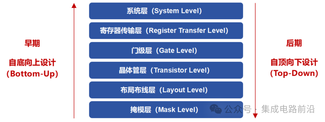 In simple terms, this means starting not from the details, but from the macro perspective—first doing system-level design, then RTL-level design (logical function design). Once the upper-level design is complete, the lower-level design (gate level, transistor level, layout and routing level, and mask level) is performed to refine every detail.The Top-Down design concept remains mainstream today. For increasingly complex chip architectures, this approach offers higher efficiency, shorter design cycles, and lower design costs.Hierarchical design, accompanied by hierarchical simulation and verification, also results in a high success rate for this design method.█ Chip Design ToolsTo achieve efficient chip design, one cannot rely solely on manual work.In the 1970s, with the continuous maturation of computer technology, chip design gradually transitioned from manual design to computer-aided design (CAD), leading to the emergence of ICCAD (IC Computer Aided Drafting).
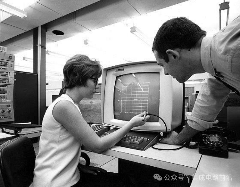 Early CAD (1967)By the 1980s, CAE (Computer Aided Engineering) emerged.CAD focuses on product design modeling and drawing, while CAE emphasizes engineering simulation and performance optimization.Later, the well-known EDA (Electronic Design Automation) was born.
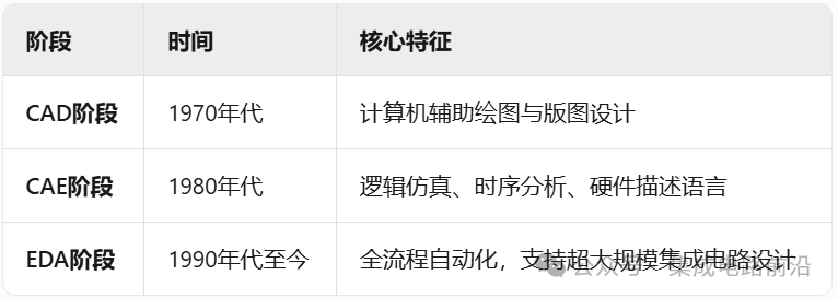 The Evolution of EDA TechnologyIt is important to note that EDA is not a specific software but a category of software. It is used not only for chip design, verification, and simulation but also for the manufacturing process of chips.In other words, EDA spans the entire R&D and production cycle of chips, helping engineers complete a large number of detailed tasks, significantly improving design efficiency, accuracy, and success rates.
 Many people are aware of photolithography machines and know that they are a key point where we are “choked”. In fact, in the EDA field, we are also “choked”, and the problem is equally serious.
Globally, the top three companies in the EDA industry are—Synopsys, Cadence, and Siemens EDA (formerly Mentor).
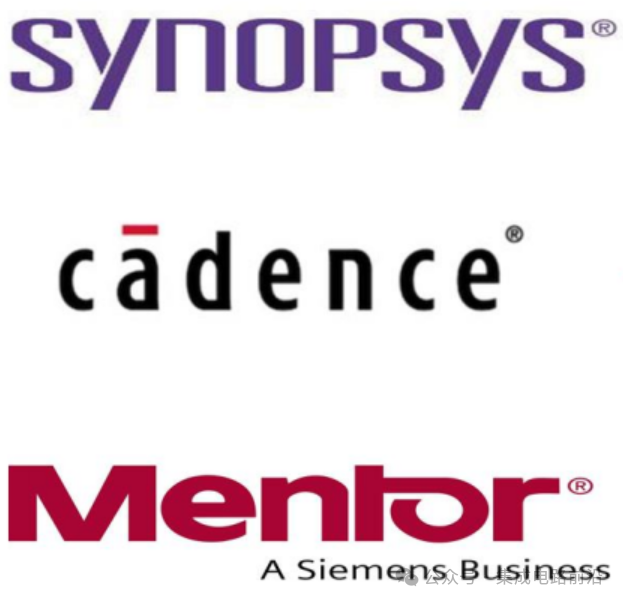
All three were founded in the 1980s in the United States and currently have a complete, full-process EDA product system, with a market share exceeding 70%, showing a significant competitive advantage.
Although there are some EDA companies in China, such as Huada Empyrean, their market share is small, and the gap with the top tier is considerable.
Recently, there was news that the US is again taking action against us in the EDA field, which is also a troublesome matter.█ Cost Investment in Chip DesignIn previous articles, I introduced that chip R&D and manufacturing have very clear divisions of labor.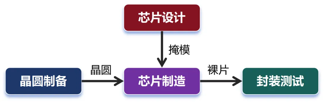 Except for a few companies (IDM, Integrated Device Manufacturers) that handle design, manufacturing, and packaging testing, most companies only do one part (Fabless, Foundry, OSAT), or a more specialized field.
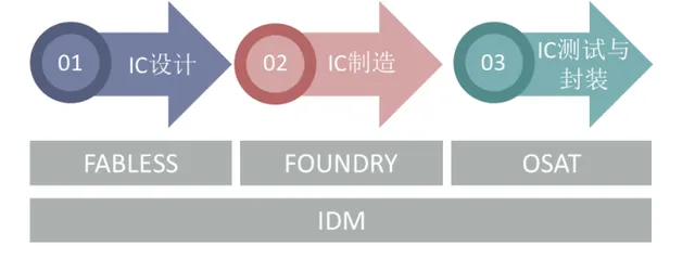 Many well-known chip companies in China, such as Huawei HiSilicon, ZTE Microelectronics, and Cambricon, are Fabless (waferless chip design companies). Recently, Xiaomi released its own mobile phone SoC chip—Xuanjie O1. They are also Fabless, only responsible for design, while the chip manufacturing is entrusted to TSMC (3nm process).The difficulty of chip design is determined by the type, function, and performance of the chip.Digital chips process digital signals and can often be produced at a large scale, especially now with many CPU, GPU, NPU computing chips, and mobile phone SoC chips, which have extremely complex structures, a high number of transistors, and significant design challenges, leading to very high costs.Designing such high-end chips often requires hundreds or even thousands of specialized technical teams, taking one to several years and investing hundreds of millions to billions of dollars. The more advanced the chip process technology, the higher the cost.
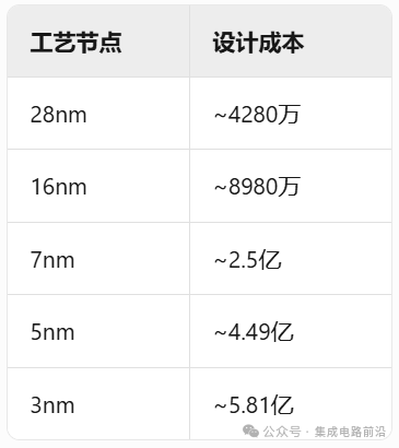 Estimated Chip Design Costs (in USD) for Reference
The costs include salaries for specialized personnel (chip design talent is highly compensated), licensing fees for EDA tools, procurement costs for IP cores (which will be mentioned later), equipment purchase costs, and operational expenses.
Analog/RF chips, which process analog signals, are often targeted at specific functions and are not as large-scale as the high-end digital chips mentioned earlier. There are also mixed-signal chips, such as ADC (Analog-to-Digital Converter) and DAC (Digital-to-Analog Converter), which are also aimed at specific applications. These chips are generally simpler compared to digital chips.
For simpler chips, some small to medium-sized teams, leveraging the currently comprehensive chip design software tool platforms (such as EDA) and hardware equipment, can also conduct independent designs. However, even for simple chips, the design cycle is approximately 1-1.5 years, with costs ranging from hundreds of thousands to millions.It is particularly noteworthy that chip design carries a high level of risk.If the tape-out (the final step in chip design, akin to creating a test version) fails, the losses can be substantial (100 million yuan for a single tape-out at 28nm, over 100 million USD for 7nm). The direct economic loss is just one aspect. A failed tape-out can also extend the chip R&D cycle, causing missed market opportunities.In severe cases, a failed tape-out can lead to the bankruptcy of a company.█ IP CoresChip design also has some “shortcuts”; for example, using IP cores.
IP cores, or Intellectual Property cores, represent pre-defined, verified, and reusable modular functional units.They are the basic elements for constructing large-scale integrated circuits.
In simple terms, when designing a complex chip, you do not have to start from scratch for every part; you can directly purchase IP cores for some mature or general functional units, significantly reducing the workload of chip design.
The design concept of mobile phone SoC chips actually comes from the reuse of IP cores.
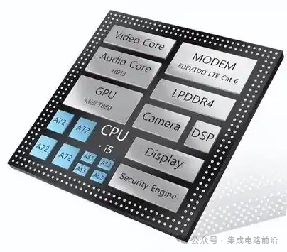
Mobile Phone SoC Chip
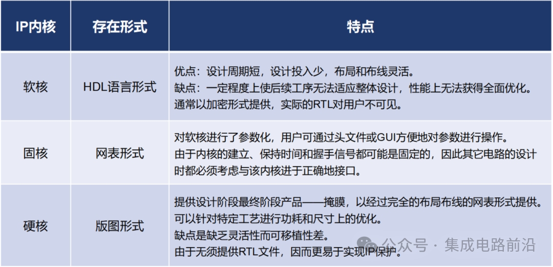
Based on characteristics, IP cores can be divided into hard cores, firm cores, and soft cores. The specific differences can be referenced in the table below:
Currently, the main market share of chip IP cores is also occupied by European and American companies, with Arm, Synopsys, and Cadence ranking in the top three.
You may have noticed that Synopsys and Cadence are the first and second of the EDA three giants mentioned earlier, right?
That’s right, bundled sales, selling software licenses and IP core licenses together yields better results and higher profits.
In the chip design industry chain, the upstream EDA tools and IP core licensing segments have gross profit margins exceeding 90%. However, these profits are primarily captured by the aforementioned companies.
Currently, the domestic localization rate of EDA tools is less than 5%, and high-end IP cores still heavily rely on imports, making the situation quite grim.
According to relevant agencies, from 2020 to 2024, the global chip design market’s compound annual growth rate is 9.8%, with the market size expected to exceed 480 billion USD by 2024. The growth in the Chinese market is even more astonishing, with its share rapidly increasing from 19% to 28%.
With the continuous advancement of digital transformation across society and the booming wave of AI, it is believed that the entire chip industry, including chip design, will continue to thrive. This presents enormous business opportunities and challenges.
That’s all for today’s article.This issue serves as a primer on the fundamentals of chip design, a sort of “appetizer”.In the next issue, we will delve into the “main course” and detail the complete process of chip design.Stay tuned!
Integrated Circuit Industry Communication Group
 Scan to join the group assistant——END——
Disclaimer: The content of this article is sourced from the internet. Except for original works, all articles, images, and related content used by this platform belong to their original rights holders. The Integrated Circuit Frontier reprints are for industry information and news sharing only and do not represent the support or endorsement of this platform for the views expressed in the article. If there are any objections or infringements, please contact the Integrated Circuit Frontier, and we will handle it promptly. Thank you!


|
The Integrated Circuit Frontier provides the latest industry news daily. Please scan the QR code below to follow us.
|