1. Experiment Task
-
Task: Based on the STEP-MAX10M08 core board and STEP BaseBoard V4.0 baseboard, complete the design of a digital barometer and observe the debugging results.
-
Requirements: Drive the digital barometer on the baseboard, displaying BMP280 information on an 8-digit scanning LED display.
-
Analysis: Use FPGA programming to drive the I2C interface of the BMP280 to obtain temperature and pressure information, then process it through BCD encoding and display it on the scanning LED display.
2.Experiment Objective
In the previous sections, we learned about the working principles and driving methods of the scanning LED display module and the BCD encoding module, as well as the I2C bus protocol and related knowledge. This experiment mainly focuses on practicing the I2C bus driving method while familiarizing ourselves with common operational methods used in FPGA design, ultimately completing the overall design of a digital temperature and humidity meter.
-
Review the working principles and communication protocols of the I2C bus.
-
Practice the I2C interface driving design method, completing the BMP280 driving design.
-
Complete the overall design of the digital temperature and humidity meter.
3.Design Block Diagram
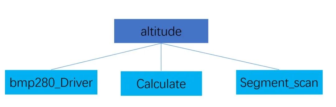
Based on the previous experiment analysis, we can see that this design can be divided into two functional modules:
-
BMP280_Driver: BMP280 chip I2C bus communication driving module.
-
Calculate: Complete the calculations, encoding, and display control from temperature and humidity code values to LED display.
-
bin_to_bcd: Method to convert binary data to BCD code.
-
Segment_scan: Display temperature and humidity data through driving the scanning LED display.
Top-Down Hierarchical Design
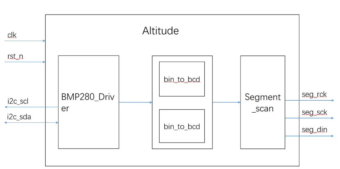
Module Structure Design
4.Experiment Principles
4.1 BMP280 Module Introduction
BMP280 is an atmospheric pressure sensor with an 8-pin 2.0mm x 2.5mm surface mount LGA package and a digital I2C bus interface. The pin function description is as follows:
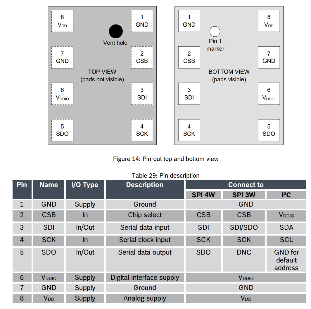
Pin Function Description
The BMP280 interface supports both I2C and SPI buses. The typical circuit for the I2C interface is as follows:

Typical Circuit Connection
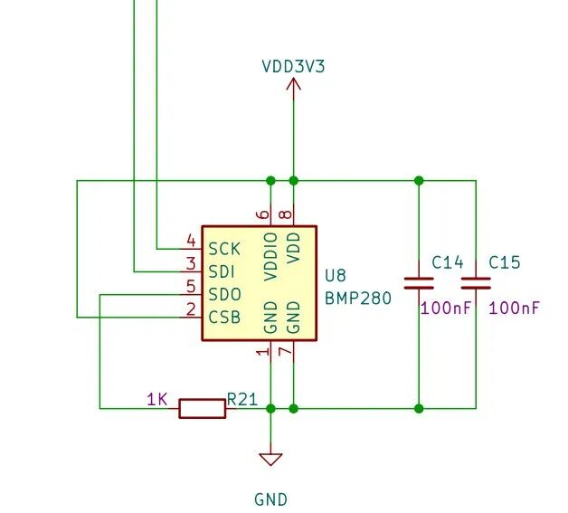
4.2 BMP280 Module Connection
The pressure sensor on the STEP BaseBoard V4.0 is connected to the BMP280 module circuit diagram below (pull-up resistors not shown):
BMP280 Module Circuit
The above diagram shows the BMP280 module circuit for the pressure sensor, which has an I2C bus (SCL, SDA) hardware interface with the FPGA. The SDO pin cannot be left floating and is used to determine the I2C device address, which can be pulled high (0x77) or low (0x76). For BMP280, both addresses are the same and can be used for I2C addressing.
4.3 BMP280 Module Driver Design
In the smart proximity system design experiment, we have already discussed the design of the I2C bus driver. This experiment can be adjusted based on the original design, starting with understanding the key parameters in the BMP280 timing.
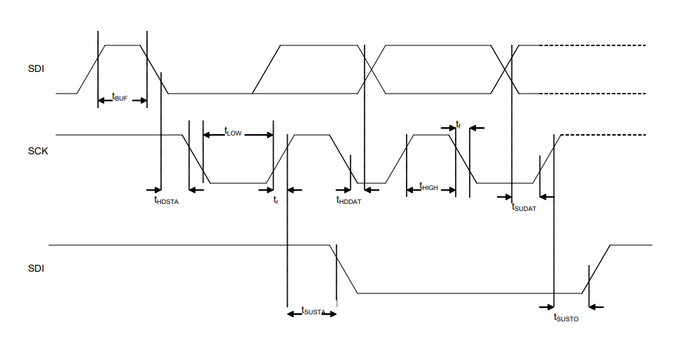
BMP280 Timing Diagram
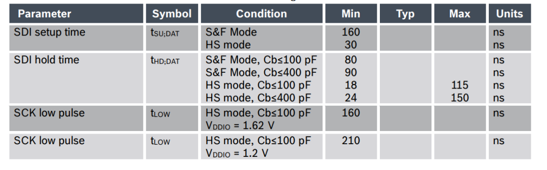
BMP280 Timing Parameters
From the BMP280 timing parameters, we understand that BMP280 supports I2C high-speed mode,
-
Dividing to obtain a clock of 400 kHz, the program implementation is the same as in the smart proximity system design experiment.
The basic units of the I2C timing protocol (start, stop, send, receive, acknowledge, read acknowledge) are unified, so the design of the basic unit states does not need to be adjusted.
-
The start timing state design program is implemented the same as in the smart proximity system design experiment.
-
The send unit and read acknowledge unit are combined, and the timing state design program is implemented the same as in the smart proximity system design experiment.
-
The receive unit and write acknowledge unit are combined, and the timing state design program is implemented the same as in the smart proximity system design experiment.
-
The stop timing state design program is implemented the same as in the smart proximity system design experiment.
When measuring, BMP280 first measures temperature, then measures pressure, checks if filtering calculations are needed, and finally stores the results in registers. During driving, first perform a software reset, then set the configuration register, and then read the data.
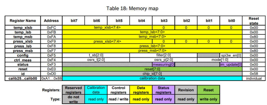
Configuration Register
This experiment involves software reset, temperature and pressure measurement, reading configuration parameters, and reading data.
Software Reset:
The I2C write operation timing: the software reset operation register is 0xE0, writing the value 0xB6 to the register completes the device reset. Similarly, registers 0xF4 and 0xF5 also need to be configured, and specific parameters can be referenced in the data sheet.
We design this operation as a state, and the program implementation is as follows:
MODE1:begin //16-bit register write operationif(cnt_mode1 >= 4'd5) cnt_mode1 <= 1'b0; // Control execution of the sub-state in STARTcnt_start else cnt_mode1 <= cnt_mode1 + 1'b1; state_back <= MODE1; case(cnt_mode1) 4'd0: begin state <= START; end //START in I2C communication timing 4'd1: begin data_wr <= dev_addr<<1; state <= WRITE; end //Device address 4'd2: begin data_wr <= reg_addr[15:8]; state <= WRITE; end //Register address 4'd3: begin data_wr <= reg_addr[7:0]; state <= WRITE; end //Register address 4'd4: begin state <= STOP; end //STOP in I2C communication timing 4'd5: begin state <= MAIN; end //Return to MAIN default: state <= IDLE; //If the program is out of control, enter IDLE self-reset state endcaseendCompensation Parameter Reading:
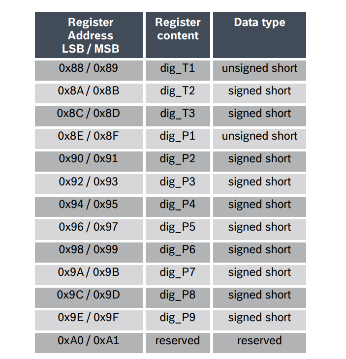
The chip internally has NVM non-volatile memory that stores a series of parameters for compensation calculations, which are written at the factory and cannot be modified, used for calculating measured temperature and pressure values. First, we need to read these parameters:
I2C Read Operation:
Reading parameters is completed using two consecutive read operations, and the program implementation is as follows:
MODE2:begin //Two read operations if(cnt_mode2 >= 4'd10) cnt_mode2 <= 1'b0; else cnt_mode2 <= cnt_mode2 + 1'b1; state_back <= MODE2; case(cnt_mode2) 4'd0: begin state <= START; end //START in I2C communication timing 4'd1: begin data_wr <= dev_addr<<1; state <= WRITE; end //Device address 4'd2: begin data_wr <= reg_addr; state <= WRITE; end //Register address 4'd3: begin state <= START; end //START in I2C communication timing 4'd4: begin data_wr <= (dev_addr<<1)|8'h01; state <= WRITE; end //Device address 4'd5: begin ack <= ACK; state <= READ; end //Read register data 4'd6: begin dat_l <= data_r; end 4'd7: begin ack <= NACK; state <= READ; end //Read register data 4'd8: begin dat_h <= data_r; end 4'd9: begin state <= STOP; end //STOP in I2C communication timing 4'd10: begin state <= MAIN; end //Return to MAIN default: state <= IDLE; //If the program is out of control, enter IDLE self-reset state endcaseend Finally, we program the control state machine to run according to the driving routine code, and the program implementation is as follows:
MAIN:begin if(cnt_main >= 4'd4) cnt_main <= 4'd2; //After writing control instructions, loop to read data else cnt_main <= cnt_main + 1'b1; case(cnt_main) 4'd0: begin dev_addr <= 7'h44; reg_addr <= 16'h30a2; state <= MODE1; end //Software reset 4'd1: begin num_delay <= 24'd600; state <= DELAY; end //1.5ms delay 4'd2: begin dev_addr <= 7'h44; reg_addr <= 16'h2c06; state <= MODE1; end //Write configuration 4'd3: begin num_delay <= 24'd6000; state <= DELAY; end //15ms delay 4'd4: begin dev_addr <= 7'h44; state <= MODE2; end //Read configuration default: state <= IDLE; //If the program is out of control, enter IDLE self-reset state endcaseendMeasurement Data Reading:
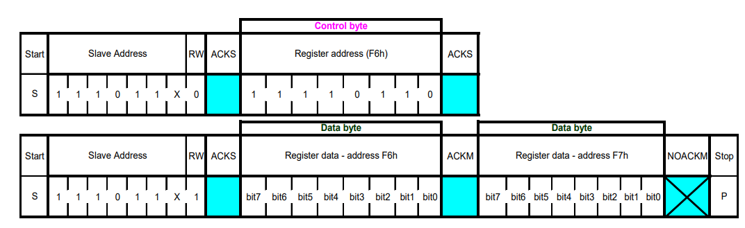
The temperature and pressure measurement data of BMP280 are stored in three bytes, and reading data is completed using three consecutive read operations, and the program implementation is as follows:
MODE3:begin //Three read operations if(cnt_mode3 >= 4'd12) cnt_mode3 <= 1'b0; //Control execution of the sub-state in STARTcnt_start else cnt_mode3 <= cnt_mode3 + 1'b1; state_back <= MODE3; case(cnt_mode3) 4'd0: begin state <= START; end //START in I2C communication timing 4'd1: begin data_wr <= dev_addr<<1; state <= WRITE; end //Device address 4'd2: begin data_wr <= reg_addr; state <= WRITE; end //Register address 4'd3: begin state <= START; end //START in I2C communication timing 4'd4: begin data_wr <= (dev_addr<<1)|8'h01; state <= WRITE; end //Device address 4'd5: begin ack <= ACK; state <= READ; end //Read register data 4'd6: begin dat_h <= data_r; end 4'd7: begin ack <= ACK; state <= READ; end //Read register data 4'd8: begin dat_l <= data_r; end 4'd9: begin ack <= NACK; state <= READ; end //Read register data 4'd10: begin dat_xl <= data_r; end 4'd11: begin state <= STOP; end //STOP in I2C communication timing 4'd12: begin state <= MAIN; end //Return to MAIN default: state <= IDLE; //If the program is out of control, enter IDLE self-reset state endcaseendFinally, we program the control state machine to run according to the driving routine code, and the program implementation is as follows:
MAIN:begin if(cnt_main >= 8'd34) cnt_main <= 8'd28; //After writing control instructions, loop to read data else cnt_main <= cnt_main + 1'b1; case(cnt_main) 8'd0: begin dev_addr <= 7'h76; reg_addr <= 8'hE0; reg_data <= 8'hb6; state <= MODE1; end //Write configuration 8'd1: begin state <= DELAY; end //200ms delay 8'd2: begin dev_addr <= 7'h76; reg_addr <= 8'hf4; reg_data <= 8'h55; state <= MODE1; end //Write configuration 8'd3: begin dev_addr <= 7'h76; reg_addr <= 8'hf5; reg_data <= 8'h00; state <= MODE1; end //Write configuration 8'd4: begin dev_addr <= 7'h76; reg_addr <= 8'h88; state <= MODE2; end //Read configuration 8'd5: begin dig_t1 <= {dat_h,dat_l}; end //Read data 8'd6: begin dev_addr <= 7'h76; reg_addr <= 8'h8a; state <= MODE2; end //Read configuration 8'd7: begin dig_t2 <= {dat_h,dat_l}; end //Read data 8'd8: begin dev_addr <= 7'h76; reg_addr <= 8'h8c; state <= MODE2; end //Read configuration 8'd9: begin dig_t3 <= {dat_h,dat_l}; end //Read data 8'd10: begin dev_addr <= 7'h76; reg_addr <= 8'h8e; state <= MODE2; end //Read configuration 8'd11: begin dig_p1 <= {dat_h,dat_l}; end //Read data 8'd12: begin dev_addr <= 7'h76; reg_addr <= 8'h90; state <= MODE2; end //Read configuration 8'd13: begin dig_p2 <= {dat_h,dat_l}; end //Read data 8'd14: begin dev_addr <= 7'h76; reg_addr <= 8'h92; state <= MODE2; end //Read configuration 8'd15: begin dig_p3 <= {dat_h,dat_l}; end //Read data 8'd16: begin dev_addr <= 7'h76; reg_addr <= 8'h94; state <= MODE2; end //Read configuration 8'd17: begin dig_p4 <= {dat_h,dat_l}; end //Read data 8'd18: begin dev_addr <= 7'h76; reg_addr <= 8'h96; state <= MODE2; end //Read configuration 8'd19: begin dig_p5 <= {dat_h,dat_l}; end //Read data 8'd20: begin dev_addr <= 7'h76; reg_addr <= 8'h98; state <= MODE2; end //Read configuration 8'd21: begin dig_p6 <= {dat_h,dat_l}; end //Read data 8'd22: begin dev_addr <= 7'h76; reg_addr <= 8'h9a; state <= MODE2; end //Read configuration 8'd23: begin dig_p7 <= {dat_h,dat_l}; end //Read data 8'd24: begin dev_addr <= 7'h76; reg_addr <= 8'h9c; state <= MODE2; end //Read configuration 8'd25: begin dig_p8 <= {dat_h,dat_l}; end //Read data 8'd26: begin dev_addr <= 7'h76; reg_addr <= 8'h9e; state <= MODE2; end //Read configuration 8'd27: begin dig_p9 <= {dat_h,dat_l}; end //Read data 8'd28: begin dev_addr <= 7'h76; reg_addr <= 8'hf4; reg_data <= 8'h55; state <= MODE1; end //Write configuration 8'd29: begin state <= DELAY; dat_valid <= 1'b0; end //200ms delay 8'd30: begin dev_addr <= 7'h76; reg_addr <= 8'hf7; state <= MODE3; end //Read configuration 8'd31: begin adc_p <= {dat_h,dat_l,dat_xl[7:4]}; end //Read data 8'd32: begin dev_addr <= 7'h76; reg_addr <= 8'hfa; state <= MODE3; end //Read configuration 8'd33: begin adc_t <= {dat_h,dat_l,dat_xl[7:4]}; end //Read data 8'd34: begin dat_valid <= 1'b1; end //Read data default: state <= IDLE; //If the program is out of control, enter IDLE self-reset state endcaseend4.4 Overall System Implementation
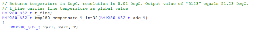
The BMP280 driver module obtains the encoded values of temperature and pressure, which still need compensation calculations to obtain the actual temperature and pressure values. The calculated data is in binary form, and to display it on the LED display, BCD encoding is required.
As can be seen, there are many multiplication operations in the formula. To make better use of board resources, we generally do not directly use the “*” symbol, but instead use appropriate multipliers based on actual conditions. The multiplier we use is as follows:
module multiply( // Multiplier input clk, // Clock input mult_begin, // Multiplication start signal input [31:0] mult_op1, // Multiplicand 1 input [31:0] mult_op2, // Multiplicand 2 output [63:0] product, // Product output mult_end // Multiplication end signal); //Multiplication in progress signal and end signal reg mult_valid; //Load multiplier, during operation shift right once, equivalent to y reg [31:0] multiplier; assign mult_end = mult_valid & ~(|multiplier); //Multiplication end signal: multiplier all 0 always @(posedge clk) //① begin if (!mult_begin || mult_end) //If not started or already ended begin mult_valid <= 1'b0; //mult_valid assigned to 0, indicating no effective multiplication operation is currently taking place end else begin mult_valid <= 1'b1; // test <= 1'b1; end end //Two source operands take absolute values, the absolute value of a positive number is itself, the absolute value of a negative number is its negation plus 1 wire op1_sign; //Sign bit of operand 1 wire op2_sign; //Sign bit of operand 2 wire [31:0] op1_absolute; //Absolute value of operand 1 wire [31:0] op2_absolute; //Absolute value of operand 2 assign op1_sign = mult_op1[31]; assign op2_sign = mult_op2[31]; assign op1_absolute = op1_sign ? (~mult_op1+1) : mult_op1; assign op2_absolute = op2_sign ? (~mult_op2+1) : mult_op2; //Load multiplicand, during operation shift left once reg [63:0] multiplicand; always @ (posedge clk) //② begin if (mult_valid) begin // If multiplication is in progress, shift multiplicand left by one each clock multiplicand <= {multiplicand[62:0],1'b0}; //Multiplicand x shifts left by one each time. end else if (mult_begin) begin // Multiplication starts, load multiplicand, which is the absolute value of multiplicand 1 multiplicand <= {32'd0,op1_absolute}; end end always @ (posedge clk) //③ begin if(mult_valid) begin //If multiplication is in progress, shift multiplier right by one each clock multiplier <= {1'b0,multiplier[31:1]}; //Equivalent to shifting multiplier y right by one end else if(mult_begin) begin //Multiplication starts, load multiplier, which is the absolute value of multiplicand 2 multiplier <= op2_absolute; end end // Partial product: if the last bit of the multiplier is 1, it is obtained by shifting the multiplicand left; if the last bit of the multiplier is 0, the partial product is 0 wire [63:0] partial_product; assign partial_product = multiplier[0] ? multiplicand:64'd0; //If the lowest bit of y is 1, assign x to partial_product; otherwise assign 0 to partial_product //Accumulator reg [63:0] product_temp; //Temporary result always @ (posedge clk) //④//clk signal changes from 0 to 1, triggers the execution of this statement, but the execution of the statement takes time begin if (mult_valid) begin product_temp <= product_temp + partial_product; end else if (mult_begin) begin product_temp <= 64'd0; end end //Sign bit of multiplication result and multiplication result reg product_sign; //Sign of product result always @ (posedge clk) // ⑤ begin if (mult_valid) begin product_sign <= op1_sign ^ op2_sign; end end //If the multiplication result is negative, the result needs to be negated +1 assign product = product_sign ? (~product_temp+1) : product_temp;endmodule Similarly, for the division in the formula, we will also use the following divider for calculations:
module div32( input clk,rst_n, input start, input [31:0] a, input [31:0] b, output done, output [31:0] yshang, output [31:0] yyushu); reg[63:0] temp_a;reg[63:0] temp_b;reg[5:0] cnt;reg done_r; reg start_last;wire start_flag_w; reg [3:0] state_c;parameter IDLE = 4'b1111;parameter INIT = 4'b0001;parameter CAL1 = 4'b0010;parameter CAL2 = 4'b0100;parameter DONE = 4'b1000; always@(posedge clk or negedge rst_n)begin if(!rst_n) begin start_last <= 1'b0; end else begin start_last <= start; endend assign start_flag_w = (~start_last)& (start); always@(posedge clk or negedge rst_n)begin if(!rst_n) begin state_c <= IDLE; end else begin case (state_c) IDLE : state_c <= (start_flag_w)?INIT:IDLE; INIT : state_c <= CAL1; CAL1 : state_c <= CAL2; CAL2 : state_c <= (cnt == 6'd31)?DONE:CAL1; DONE : state_c <= IDLE; default: state_c <= IDLE; endcase endend//------------------------------------------------always @(posedge clk or negedge rst_n)begin if(!rst_n) cnt <= 6'd0; else if (state_c == INIT) cnt <= 6'd0; else if (state_c == CAL2) cnt <= cnt + 1; else cnt <= cnt;end//------------------------------------------------ assign done = (state_c == DONE)?1'b1:1'b0;//------------------------------------------------always @(posedge clk or negedge rst_n)begin if(!rst_n) begin temp_a <= 64'h0; temp_b <= 64'h0; end else begin case (state_c) IDLE: begin temp_a <= 64'h0; temp_b <= 64'h0; end INIT: begin temp_a <= {32'h00000000,a}; temp_b <= {b,32'h00000000}; end CAL1: begin temp_a <= temp_a << 1; end CAL2: begin if (temp_a[63:32] > temp_b[63:32]) begin temp_a <= temp_a -temp_b + 1; end else temp_a <= temp_a; end default: begin temp_a <= temp_a; temp_b <= temp_b; end endcase endendassign yshang = temp_a[31:0];assign yyushu = temp_a[63:32];endmoduleCalculation counter, used to determine the calculation steps, since addition, subtraction, and shifting operations take different times than multiplication and division, the counter should be incremented based on the calculation mode.
reg [5:0] cnt_cal; //Formula counterreg [1:0] cal_mode;//00 sim_cal, 01 mult; 11 div;wire mult_end;//Multiplication end signal;wire div_done_w;//Division end signal;always@(posedge clk or negedge rst_n)begin if(!rst_n) begin cnt_cal <= 6'b0; end else if (cnt_cal == 51) begin cnt_cal <= 'd0; end else begin case (cal_mode) MUL:begin if (mult_end) begin cnt_cal <= cnt_cal + 1'b1; end else begin cnt_cal <= cnt_cal; end end DIV:begin if (div_done_w) begin cnt_cal <= cnt_cal + 1'b1; end else begin cnt_cal <= cnt_cal; end end SIM:begin cnt_cal <= (cnt_sync)? cnt_cal + 1'b1:cnt_cal; end default: cnt_cal <= cnt_cal; endcase endendObtain BMP280 compensation data for calculations:
reg signed [15:0] digP1,digP2,digP3,digP4,digP5,digP6,digP7,digP8,digP9;reg signed [15:0] digp;always@(posedge dat_valid)begin digP1 <= dig_p1; digP2 <= dig_p2; digP3 <= dig_p3; digP4 <= dig_p4; digP5 <= dig_p5; digP6 <= dig_p6; digP7 <= dig_p7; digP8 <= dig_p8; digP9 <= dig_p9;endalways@(posedge clk)begin case (cnt_cal) 'd13: digp <= (digP6[15]) ? (~digP6 + 1'b1) : digP6; 'd15: digp <= (digP5[15]) ? (~digP5 + 1'b1) : digP5; 'd17: digp <= (digP4[15]) ? (~digP4 + 1'b1) : digP4; 'd20: digp <= (digP3[15]) ? (~digP3 + 1'b1) : digP3; 'd22: digp <= (digP2[15]) ? (~digP2 + 1'b1) : digP2; 'd25: digp <= digP1; 'd28: adcp <= adc_p; 'd40: digp <= (digP9[15]) ? (~digP9 + 1'b1) : digP9; 'd43: digp <= (digP8[15]) ? (~digP8 + 1'b1) : digP8; 'd45: digp <= (digP7[15]) ? (~digP7 + 1'b1) : digP7; default: begin adcp <= adcp; digp <= digp; end endcaseendThus, we can calculate the pressure value based on the calculation formula, for example, var2 = (((var1>>2) * (var1>>>2)) >> 11) * ((BMP280_S32_t)dig_P6).
'd12 :begin cal_mode <= MUL; mult_op1 <= var1 >>> 2; mult_op2 <= var1 >>> 2; end 'd13 :begin cal_mode <= SIM; var2 <= (cnt_sync)?var2:(product >>> 11); end 'd14 :begin cal_mode <= MUL; mult_op1 <= var2; mult_op2 <= {16'd0,digp}; end 'd15:begin cal_mode <= SIM; var2 <= (cnt_sync)?var2:product[31:0]; endBCD encoding was introduced in the previous voltage regulator experiment and can be instantiated directly.
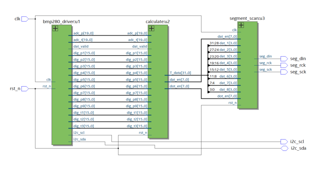
The comprehensive design block diagram is as follows:
5.Experiment Steps
(1) Double-click to open the Quartus Prime software;
(2) Create a new project: File → New Project Wizard (Project naming, project directory selection, device model selection, EDA tool selection);
(3) Create a new file: File → New → Verilog HDL File, type the design code and save;
(4) Design synthesis: Double-click Tasks window page under Analysis & Synthesis to synthesize the code;
(5) Pin constraints: Assignments → Assignment Editor, assign pins according to project requirements;
(6) Design compilation: Double-click Tasks window page under Compile Design to compile the design and generate configuration files;
(7) Program burning: Click Tools → Programmer to open the configuration tool, Program to download;
(8) Observe the design running results.
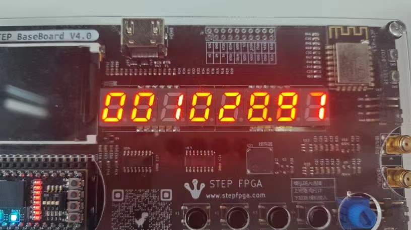
6.Experiment Phenomena
Load the program onto the FPGA, observe the LED display, which shows the temperature values measured by the BMP280.