In embedded systems, when communication is required between microcontrollers with different supply voltages, or between a microcontroller and peripheral chips operating at different voltages, level conversion is unavoidable. Otherwise, communication may fail, or the voltage may exceed the microcontroller’s tolerance, causing damage. Below are five mainstream level conversion solutions.
1. Resistor Divider Solution
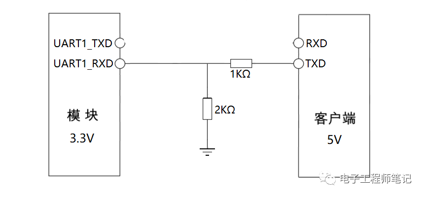
As shown in the figure above, the left side is a 3.3V system, and the right side is a 5V system. When the 5V level client sends data to the left side, the voltage at the left receiving end is approximately 5V*2K/(1K+2K)≈3.3V through two resistors, thus achieving level matching.
Since only resistors are used, the advantage of this solution is its extremely low cost and ease of layout. However, the drawbacks are quite obvious: on one hand, the power consumption is relatively high, and on the other hand, the driving capability is weak, and the speed cannot be too fast; it generally can only be applied at frequencies below 100K.
2. Level Shifter Chip Solution
Using dedicated level shifting chips, simply provide different voltages on both sides of the chip, and the level conversion is completed internally by the chip. For example, the 74xHC series and 74xHCT series chips can achieve seven-channel 3.3V to 5V level conversion.
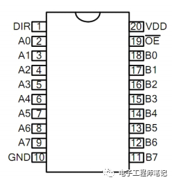
The advantage of directly using chips for level conversion is strong driving capability (CMOS output technology), low leakage current, suitability for multi-channel level conversion, and high speed. The downside is the high cost.
3. Diode Solution
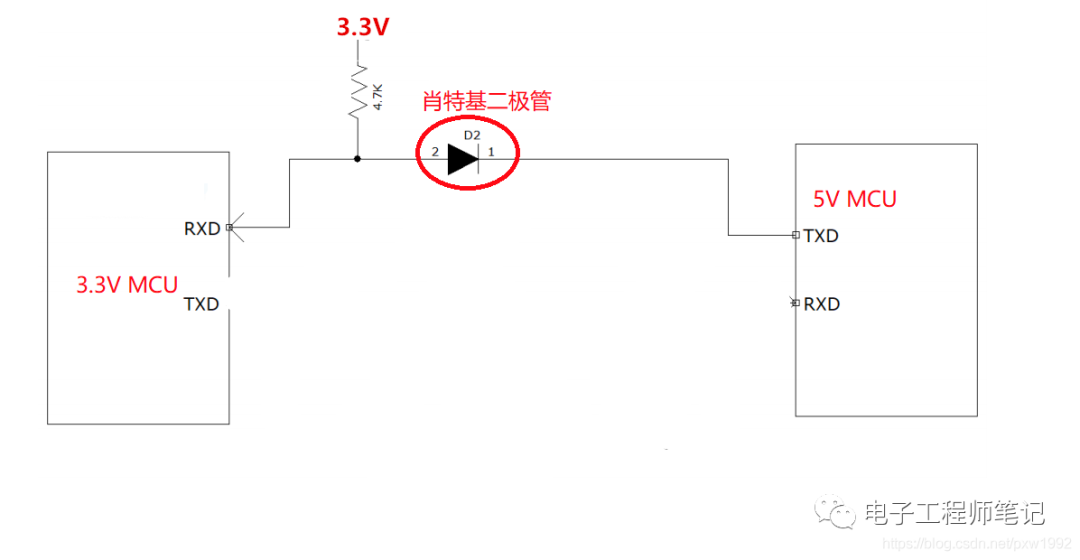
Using the voltage drop of a diode for clamping can also achieve level conversion. As shown in the figure, when the right side 5V microcontroller’s TXD outputs a high level, D2 is off, and the left side RXD receives a high level of 3.3V through a pull-up resistor; when the right side microcontroller’s TXD is low, due to the clamping effect of the diode, the left side RXD is approximately 0.3V, defaulting to low level. This circuit requires D2 to have a particularly small voltage drop (<0.5V), usually using Schottky diodes; otherwise, the levels on both sides cannot maintain consistency.
The advantages of the diode solution are low leakage current and low cost, while the downsides include high voltage drop requirements and limited driving capability and transmission speed.
4. Transistor Solution
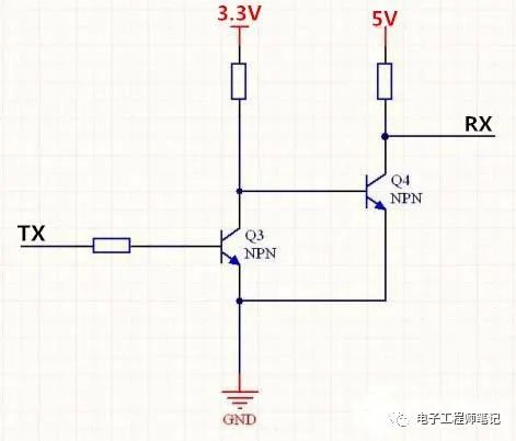
The circuit in the figure uses two NPN transistors to convert the input signal of 3.3V level to a 5V output level while keeping the signals synchronized. Circuit description: When TX is low, Q3 is off, and Q4 is on, making RX low as well; when TX is high, Q3 is on, Q4 is off, and RX is pulled up to 5V. Thus, both levels are synchronized, and level conversion is achieved.
The advantages of this circuit are low cost, strong driving capability, and mature widespread application. The downside is that the waveform has a delay when converted through transistors, so the speed cannot be too fast (baud rate should not exceed 230400). For multi-channel conversions, more materials are required, necessitating a larger layout space.
5. MOSFET Solution
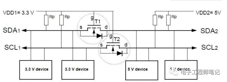
The above figure shows a classic circuit for level conversion between 5V and 3.3V in IIC communication using MOSFETs. Circuit description: When SDA1 is high, there is no voltage drop across the MOSFET G-S, so it is off, and both SDA1 and SDA2 are high, but the voltages are independent; when SDA1 is low, the MOSFET turns on, and both SDA1 and SDA2 are low. The SCL logic is similar to SDA.
This solution is suitable for low-frequency signal level conversion, is inexpensive, and has a smaller voltage drop compared to transistors, with speeds generally below 400K.
Recommended Reading:
Life Is Like Designing PCB~
A Rare Complete Guide to Component Selection