IntroductionRecently, the China Semiconductor Industry Association issued an “Emergency Notice on the Rules for Determining the ‘Place of Origin’ of Semiconductor Products,” sparking widespread discussion.The “Emergency Notice on the Rules for Determining the ‘Place of Origin’ of Semiconductor Products” states that according to the relevant regulations of the General Administration of Customs, the place of origin for “integrated circuits” is determined based on the four-digit tariff number change principle, meaning the wafer fabrication location is recognized as the place of origin. Please take note!Additionally, the China Semiconductor Industry Association recommends that the place of origin for “integrated circuits,” whether packaged or unpackaged, should be declared based on the location of the “wafer fabrication factory” during import customs clearance.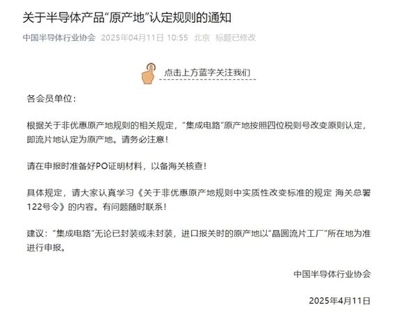 The full text of the notice is as followsTo all member units:According to the relevant regulations of the General Administration of Customs, the place of origin for “integrated circuits” is determined based on the four-digit tariff number change principle, meaning the wafer fabrication location is recognized as the place of origin. Please take note!Please prepare the PO proof materials for customs verification during declaration!For specific regulations, please study the content of the “Regulations on Substantial Change Standards in Non-Preferential Origin Rules, General Administration of Customs Order No. 122” carefully. If you have any questions, feel free to contact us!Recommendation: For “integrated circuits,” whether packaged or unpackaged, the place of origin during import customs clearance should be declared based on the location of the “wafer fabrication factory.”China Semiconductor Industry AssociationApril 11, 2025The core content of this notice can be summarized in one sentence: “the wafer fabrication location is recognized as the place of origin.” What does this actually mean?The semiconductor industry chain can be simply divided into four stages: design, manufacturing, packaging/testing, and end application, with wafer fabrication belonging to the manufacturing stage.Wafer manufacturing (fabrication) is the most critical and technically demanding stage, directly determining the chip’s process technology.Han Juke, Vice President of the China Communications Industry Association, stated that using the wafer fabrication location as the place of origin allows for a more accurate identification of the true technological source of the chip, avoiding the ambiguity of key technology attribution through the packaging location (usually labor-intensive regions).At the same time, this move is a key step in the strategy for a self-controllable semiconductor industry chain in China, aligning with international trade rules while providing institutional support for domestic industry upgrades. In the future, as the data on places of origin accumulates, China’s policy formulation and market regulation in the semiconductor field will become more targeted.Source: Kuai Technology,China Semiconductor Industry Association
-END-
Past Issues Review
REVIEW
Yushu Robotics Achieves Major Breakthrough! First Showcase of Side Flip Challenge Officially Invites Everyone to Participate
First Exposure of Beautiful Humanoid Robot Prototype: Impressive Dexterous Hand Operations
6G Included in Government Work Report! Ministry of Industry and Information Technology Reveals 6G R&D Timeline


Smart Manufacturing in the Era of Industry 4.0
“Internet +” Service Platform
Smart Manufacturing Live | Smart Manufacturing Classroom | Exhibition Cooperation
0571-89719789