Click the title below “RF Flower Pool” to quickly follow the public account!
To reduce parasitic signals in RF circuit layout, RF engineers need to be creative. Remember these eight rules, which not only help accelerate product launch but also improve the predictability of work schedules.
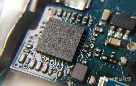
Rule 1: Ground vias should be located at the switch of the ground reference layer
All current flowing through the routed lines has equal return paths. There are many coupling strategies, but return paths usually flow through adjacent ground layers or ground arranged parallel to signal lines. When continuing in the reference layer, all coupling is limited to transmission lines, and everything is normal. However, if the signal line switches from the top layer to an internal or bottom layer, the return path must also have a route.
Figure 1 is an example. The current of the top-layer signal line is adjacent to the return path. When it shifts to the bottom layer, the return flows through nearby vias. However, if there are no nearby vias for return, the return must go through the nearest available ground via. Greater distances create current loops, forming inductors. If this unnecessary current path deviates and happens to cross another line, interference will be worse. This current loop actually forms an antenna!
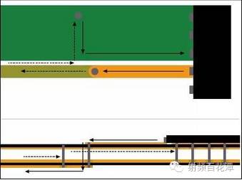
Figure 1: Signal current flows from the device pin through the via to a lower layer. The return is below the signal before being forced to flow to the nearest via to change to a different reference layer.
Ground reference is the best strategy, but high-speed lines can sometimes be placed on internal layers. It is very difficult to place ground reference layers above and below; semiconductor manufacturers may be limited by pin placement, placing power lines next to high-speed lines. If reference current needs to switch between non-DC coupled layers or nets, decoupling capacitors should be placed close to the switch points.
Rule 2: Connect device pads to the top layer ground
Many devices use thermal ground pads at the bottom of the device package. On RF devices, these are usually electrical grounds, with adjacent pads having ground via arrays. Device pads can be directly connected to ground pins and connected to any copper pours through the top layer ground. With multiple paths, return will split according to the impedance ratio of the paths. Grounding through pads is shorter and has lower impedance compared to pin grounding.
A good electrical connection between the PCB and device pads is crucial. During assembly, unfilled vias in the PCB via array may also extract solder paste from the device, leaving gaps. Filling vias is a good way to ensure proper soldering. During evaluation, also open the solder mask layer to confirm there is no solder mask on the PCB ground beneath the device, as the solder mask may raise the device or cause it to wobble.
Rule 3: No reference layer gaps
There are vias everywhere around the device. The power net decomposes locally for decoupling and then drops to the power layer, usually providing multiple vias to minimize inductance, increase current capacity, while controlling the bus to drop to inner layers. All these decompositions eventually get completely trapped near the device.
Each of these vias generates an exclusion zone on the inner ground layer larger than the via diameter itself, providing manufacturing gaps. These exclusion zones can easily cause interruptions in return paths. Some vias that are close to each other can form ground layer trenches, which are not visible in the top CAD view, complicating matters further. Figure 2 shows overlapping exclusion zones from two power layer vias that can create interruptions on the return path. The return can only detour around the ground layer exclusion zone, forming the now-common inductive path problem.
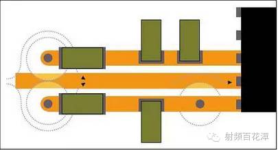
Figure 2: The exclusion zones around vias in the ground layer may overlap, forcing return paths away from signal paths. Even without overlap, exclusion zones can create impedance interruptions in the ground layer.
Even “friendly” ground vias will impose minimum size specifications required by the PCB manufacturing process on related metal pads. If vias are very close to signal lines, it will create an appearance as if the top layer ground gap has been “chewed away” by a mouse. Figure 2 illustrates the mouse bite.
Since exclusion zones are automatically generated by CAD software and vias are frequently used on system PCBs, early layout processes often encounter some return path interruption issues. During layout evaluation, track every high-speed line and check related return layers to avoid interruptions. Keeping all vias that can cause ground layer interference closer to top layer ground gaps is a good method.
Rule 4: Maintain the differential nature of differential lines
The return path is crucial to the performance of signal lines and should be considered part of the signal path. Meanwhile, differential pairs are usually not tightly coupled, and returns may flow through adjacent layers. Both returns must be routed through equal electrical paths.
Even when the two lines of a differential pair are not tightly coupled, proximity and shared design constraints may keep returns in the same layer. To truly maintain low parasitic signals, better matching is required. Any planned structure such as ground layer stoppers beneath differential components should be symmetrical. Similarly, length matching may also cause waveform curve issues in signal lines. Returns do not cause waveform curve issues. The length matching of one differential line should reflect in other differential lines.
Rule 5: No clock or control lines near RF signal lines
Clock and control lines can sometimes be seen as non-influential neighbors because of their low operating speeds, even close to DC. However, their switching characteristics are almost close to square waves, generating unique tones at odd harmonic frequencies. The fundamental frequency of square wave emissions may not have any impact, but their sharp edges can. In digital system design, the corner frequency can estimate the highest frequency harmonics that must be considered, calculated as: Fknee=0.5/Tr, where Tr is the rise time. Note that it is the rise time, not the signal frequency. However, the sharp edges of square waves also have powerful high-order odd harmonics, which may only couple onto RF lines at incorrect frequencies, violating strict transmission mask requirements.
Clock and control lines should be isolated from RF signal lines by internal ground layers or top layer ground pours. If grounding cannot isolate signals, routing should ensure right-angle crossings. This is because the magnetic flux lines emitted by clock or control lines will form radial contour lines around the current of the interference source line, which will not produce current in the receiver lines. Slowing down the rise time not only reduces the corner frequency but also helps reduce interference from interference sources, but clock or control lines can also act as receiver lines. Receiver lines can still serve as conduits for introducing parasitic signals into devices.
Rule 6: Use ground isolation for high-speed lines
Microwave transmission lines and strip lines are mostly coupled with adjacent ground layers. Some flux lines still emit horizontally and terminate on adjacent traces. A tone on a high-speed line or differential pair ends on the next trace, but ground pours on the signal layer provide a lower impedance endpoint for flux lines, preventing tone interference on adjacent traces.
Clock distribution or synthesizer device routing may be clustered together to carry the same frequency, as interference source tones already exist on receiver lines. However, clustered lines will eventually disperse. When dispersing, ground pours should be provided between dispersed lines, and vias should be poured at the point of dispersion to allow induced return to flow back along rated return paths. In Figure 3, vias at the end of the ground island provide a flow path for induced current to the reference layer. The spacing between other vias on the ground pour should not exceed one-tenth of a wavelength to ensure that grounding does not become a resonant structure.
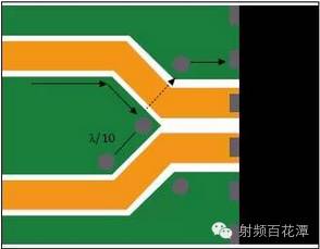
Figure 3: Top layer ground vias at the dispersion of differential lines provide flow paths for returns.
Rule 7: Do not route RF lines on noisy power layers
Tones entering the power layer will spread everywhere. If spurious tones enter power, buffers, mixers, attenuators, and oscillators, they will modulate interference frequencies. Similarly, when power reaches the PCB, it has not been thoroughly cleared to drive the RF circuit system. RF line exposure on power layers should be minimized, especially on unfiltered power layers.
Large power layers adjacent to ground can create high-quality embedded capacitors that attenuate parasitic signals and are used for digital communication systems and certain RF systems. Another method is to minimize power layers, sometimes more like thick traces rather than layers, allowing RF lines to more thoroughly avoid power layers. Both methods are feasible, but never combine the worst characteristics of both, which is to use small power layers while routing RF lines on top.
Rule 8: Place decoupling close to the device
Decoupling not only helps avoid stray noise entering the device but also helps eliminate tones generated internally by the device, preventing them from coupling onto the power layer. The closer decoupling capacitors are to the working circuit system, the more efficient they are. Local decoupling is less disturbed by the parasitic impedance of PCB traces, and shorter traces support smaller antennas, reducing harmful tone emissions. Capacitor placement should consider the highest self-resonant frequency, usually the minimum value, minimum shell size, closest to the device, and the larger the capacitor, the further from the device. At RF frequencies, capacitors on the back of the PCB can create parasitic inductance in via series connecting ground paths, losing a lot of noise attenuation advantages.
Conclusion
Through PCB layout evaluation, we can identify structures that may emit or receive stray RF tones. Track each line, consciously clarify its return path, ensuring it can parallel with the lines, especially thoroughly check transitions. Additionally, isolate potential interference sources from receivers. Following some simple intuitive rules to reduce parasitic signals can accelerate product releases and reduce debugging costs.

WeChat Group of Thousands
1. Do not join the same group repeatedly
2. Only for RF-related personnel

Add the group owner, note: unit + directionRF Flower Pool
Follow the largest RF public account in China

RF Flower Pool
Focuses on technology sharing and information dissemination in the RF microwave field. Established by senior RF expert Xu Xingfu, director of Shenzhen Xingsen Fast RF Laboratory, and editor of “ADS2008/2011 RF Circuit Design and Simulation Examples” and “HFSS RF Simulation Design Examples Collection”, this account has gained 40,000 followers and 10,000 group members, including several IEEE Fellows.
For PCB manufacturing, RF microwave/high-frequency high-speed PCB design and simulation, and technical consulting, please contact the group owner: 15989459034 [email protected].