Abstract
/
This article reviews the power supply requirements for FPGAs, emphasizing voltage accuracy, transient response, and voltage sequencing, and details various challenges related to thermal management through operational examples. It then introduces integrated DC/DC regulators from Analog Devices and evaluation boards and integrated recommendations that can accelerate the design process. These regulators are suitable for powering FPGAs, including flat versions that can be mounted on the back of PC boards.
Field Programmable Gate Arrays (FPGAs) are increasingly used to support high-performance computing in video and image processing, medical systems, automotive and aerospace applications, as well as artificial intelligence (AI) and machine learning (ML). Powering FPGAs is a complex and critical function that involves a variety of power rails, some requiring currents of up to 50 A.
To ensure proper operation of the FPGA, the power rails need to be turned on and off in a specific sequence, with monotonic rise and fall, and require high precision voltage and fast transient response capabilities. Additionally, the DC/DC regulators used to provide various voltages need to be compact to minimize parasitic effects in the distribution lines by placing them close to the FPGA. Furthermore, these power supplies must be efficient to reduce temperature rise near the FPGA. In some systems, the form factor of the DC/DC regulators must be thin enough to allow installation on the back of the printed circuit board (PCB).
While it is possible to design high-efficiency, high-performance DC/DC regulators with the necessary integrated digital power management features, meeting these requirements in a very compact, flat form factor presents a significant challenge. This can lead to countless design iterations and disrupt the FPGA system design, ultimately resulting in delayed time-to-market and reduced system performance.
To address this, FPGA power system designers can adopt well-tested, validated integrated DC/DC regulators. These regulators integrate all components within their high thermal efficiency compact Land Grid Array (LGA) and Ball Grid Array (BGA) packages, making them suitable for direct integration next to the FPGA, maximizing the performance of the power system (and the FPGA).
Power Requirements of FPGAs
/
Internal functional devices of FPGAs, such as core logic, input/output (I/O) circuits, auxiliary circuits, and transceivers, require different power rails. These regulators typically use a distributed power architecture, equipping each power rail with one or more DC/DC regulators, also known as Point of Load (POL) regulators. While most of these regulators use switch-mode power conversion for maximum efficiency, noise-sensitive circuits like transceivers may require Low Dropout (LDO) regulators.
In small systems, the distribution voltage is typically 5 V or 12 V DC, which can directly power the POL. In larger systems, the distribution voltage can be 24 V or 48 VDC. When using higher distribution voltages, buck regulators are used on the intermediate voltage bus supplying the POL to step down the distribution voltage to 5 V or 12 VDC. The POL provides the low voltage required for each FPGA power rail (Figure 1). Each power rail has specific requirements related to accuracy, transient response, sequencing, and other parameters.
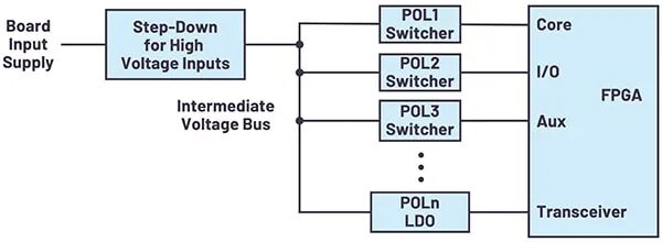
Figure 1: Powering FPGAs requires multiple POL regulators.
(Image Source: Analog Devices)
The core POL is typically the most critical power supply in an FPGA. The core power can be below 1 VDC, with currents in the tens of amperes, and usually has accuracy requirements of ±3% or higher to prevent logic errors. For example, for an FPGA with a ±3% core voltage tolerance specification, a regulator with an accuracy of ±1.5% can achieve another ±1.5% transient. If the POL has good transient response capability, reliable performance will be achieved. However, achieving the required performance with a regulator that has an accuracy of ±2% is quite challenging. Only ±1% can be used for transient response, requiring the addition of bypass capacitors, which may lead to logic errors during transients.
Sequencing Fluctuations
/
In addition to having stringent power requirements during operation, FPGAs also require various power rails to be turned on and off in a specific sequence and precise timing. Modern FPGAs typically have many power rails, managed in groups that can be turned on and off together. For example, the power domains of Intel’s Altera Arria 10 FPGA are divided into three groups for management. These groups must be powered on in the order from the first group (with six voltage rails) to the second group (also six voltage rails), and then to the third group (three voltage rails), and powered off in the reverse order to prevent damage to the FPGA (Figure 2).
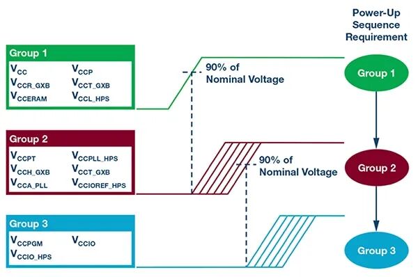
Figure 2: FPGAs require power rails to be powered on and off in a specific order.
(Image Source: Analog Devices)
Minimizing Heat Generation
/
With so many regulators located close to the FPGA, thermal management is a concern. Analog Devices has assembled a PCB to demonstrate some thermal management options when using multiple regulators (Figure 3). Thermal performance is affected by the relative position of the regulators, the direction and magnitude of airflow, and ambient temperature.
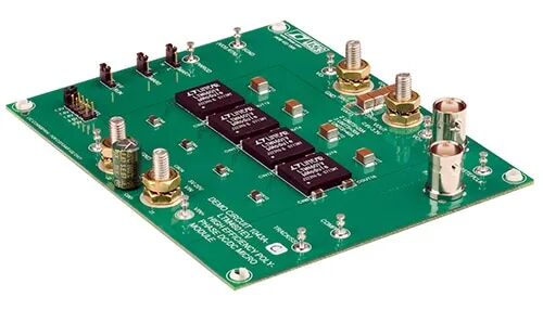
Figure 3: Thermal management demonstration board for parallel regulators.
(Image Source: Analog Devices)
For initial comparisons, seven positions on the demonstration board are used to measure temperature; positions 1 to 4 show the surface temperature of the modules, while positions 5 to 7 show the surface temperature of the PCB (Figure 4). In these two thermal images, the outer modules have lower temperatures due to more heat dissipation achieved through the three sides of the PCB area, while the middle module only dissipates heat through two sides. Airflow is also important. In the left thermal image, there is 200 LFM airflow from the bottom of the PCB, while in the right image, there is no airflow. The modules and PCB with airflow are approximately 20 °C cooler.
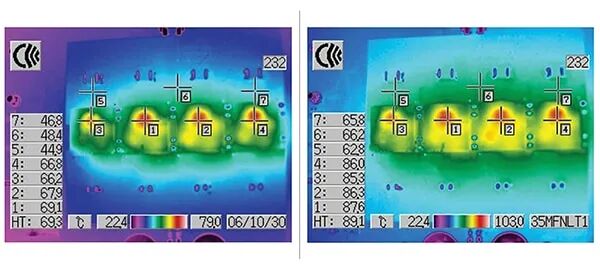 Figure 4: Increasing 200 LFM airflow can significantly lower the temperature of the modules and PCB (left).
(Image Source: Analog Devices)
The direction of airflow and ambient temperature are also important. Using 400 LFM airflow from right to left pushes heat from one module to another, resulting in the lowest temperature module being on the right, the middle module being the hottest, and the left module’s temperature being between the two (Figure 5, left). To compensate for higher ambient temperatures, heat sinks are installed on modules operating at 75 °C. Under these extreme conditions, even with added cooling devices, the module temperature rises significantly (Figure 5, right).
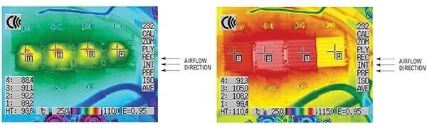
Figure 5: Effects of 50 °C (left) and 75 °C (right) ambient temperatures with 400 LFM airflow passing through the PCB.
(Image Source: Analog Devices)
LGA and BGA Packages for Back-Mounting
/
The LTM4601 series of continuous 12 A (14 A peak) buck DC/DC regulators provides designers with the option of 15 × 15 × 2.82 mm LGA or 15 × 15 × 3.42 mm BGA packages. The input voltage range for this series is 4.5 V to 20 VDC, providing output from 0.6 V to 5 VDC, with output voltage tracking and margin effects. This series features ±1.5% regulation and 35 mV peak deviation, suitable for full load dynamic changes from 0% to 50% and from 50% to 0%, with a rise time of 25 µs.
This regulator comes with and without onboard differential remote sensing amplifiers for precise output voltage adjustment, unaffected by load current. For example, the LTM4601IV#PBF comes in LGA package, while the LTM4601IY#PBF comes in BGA package, both featuring onboard differential remote sensing amplifiers. Applications that do not require onboard amplifiers can use the LGA package LTM4601IV-1#PBF device or the BGA package LTM4601IY-1#PBF device. These modules are complete DC/DC regulators that only require input and output capacitors to meet specific design requirements (Figure 6). These modules have a flat form factor, allowing them to be mounted on the back of the PCB.
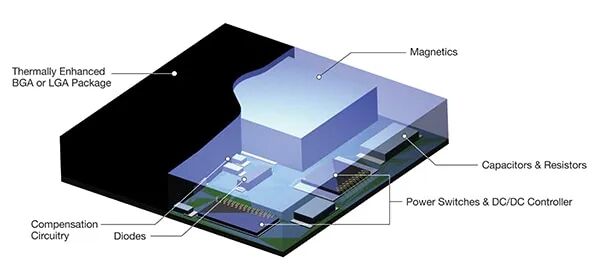
Figure 6: μModule regulators are complete power converters with thermally enhanced packaging.
(Image Source: Analog Devices)
Analog Devices offers the DC1041A-A demonstration circuit to accelerate the evaluation of the LTM4601 regulator. The input voltage range for this device is 4.5 V to 20 VDC, and the output voltage can be selected via jumpers or set to track another module’s output either precisely or proportionally.
Ultra-Thin Regulators
/
The 16 × 11.9 mm LGA package of Analog Devices’ LTM4686 has a height of 1.82 mm, allowing these dual 10 A or single 20 A regulators to be installed close enough to share heat sinks, simplifying thermal management. Additionally, these regulators are suitable for installation on the back of PC boards. Integrated digital power management features using the PMBus protocol support remote configuration and real-time monitoring of output current, voltage, temperature, and other parameters. These regulators can support two input voltage ranges; the LTM4686IV#PBF operates at 4.5 V to 17 VDC, while the LTM4686IV-1#PBF operates at 2.375 V to 17 VDC. The LTM4686 module supports output from 0.5 V to 3.6 VDC, with a maximum output error of ±0.5%. Under ambient temperatures of +85 °C, 400 LFM airflow, and 5 VDC input, these regulators can provide 1 VDC 18 A output.
Designers can combine the DC2722A demonstration circuit with LTpowerPlay software to explore the capabilities of the LTM4686 module. If only for regulator evaluation, the DC2722A can be powered on with default settings without requiring PMBus communication. After adding the software and PMBus dongle, designers can explore comprehensive digital power management capabilities, including instant reconfiguration of parts and viewing remote information.
PCB Layout Considerations
/
While electrical factors are rarely considered when powering FPGAs with parallel μModule regulators, parameters related to spacing, vias, ground planes, and airflow are crucial. Fortunately, the LGA package design simplifies the layout of power and ground planes and provides reliable thermal connections for the PCB. Placing four parallel μModule regulators is straightforward, as it replicates the footprint of the LGA (Figure 7). Except for exceptionally harsh environments, thermally enhanced packaging and power planes typically provide sufficient cooling for the modules.
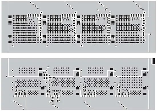
Figure 7: The LGA package of μModule regulators simplifies the parallel connection of multiple modules and supports enhanced thermal performance.
(Image Source: Analog Devices)
Conclusion
/
To support high-performance computing applications, FPGAs require precise, efficient power management and fast response times. Powering the numerous voltage rails in FPGAs is a complex challenge that can be addressed using Analog Devices’ integrated μModule DC/DC regulators. These regulators also achieve the required electrical and thermal performance in compact and easy-to-integrate packages.
Editor’s Note
/
As discussed in the article, FPGAs have a wide range of application scenarios, and powering them requires meeting various power rail and high current demands. High-quality regulators, through technical optimizations (such as high precision, fast response, thermal management) and design simplifications (such as compact packaging, easy integration), become core components of FPGA power supply systems, directly enhancing system reliability, efficiency, and market competitiveness. What type of regulator do you use in your FPGA power design? What insights or questions do you have regarding related regulators? Feel free to leave a comment and share your thoughts!
 #Regulator #FPGA #Power Chip