The integrated circuit EDA tools are not a single tool, but a collection of point tools that form a tool chain from front-end design (RTL to gate-level netlist) to back-end design (gate-level netlist to GDS), including synthesis, formal verification and simulation, logic synthesis, testability design, layout planning, placement, clock tree synthesis, routing, timing analysis optimization, electromigration voltage drop/power analysis, parasitic parameter extraction, physical verification, etc. The breakthrough of EDA tools relies on the key technological breakthroughs of various EDA point tools as well as the integration and design optimization of these point tools. Therefore, the chain of EDA point tools based on a common data foundation and the integrated optimization based on the entire EDA chain have become the only path to promote breakthroughs in EDA tools.
In view of the many challenges and opportunities facing EDA technology development, this publication has specially planned to publish the “EDA Research Column”, selecting excellent EDA technology papers from CCF-DAC 2023, covering innovative methods and key technologies in layout planning, timing analysis, routing, and other directions. Experts are welcome to submit papers and provide feedback on the construction of the EDA column. This special topic has been published in the first issue of 2024 of “Integrated Circuits and Embedded Systems”.
The four articles are as follows (click to read or download the full PDF version):
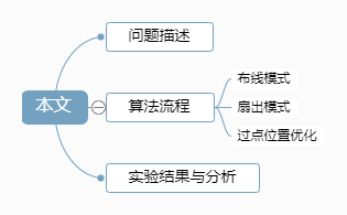
A flexible circuit board routing planning algorithm based on pattern routing
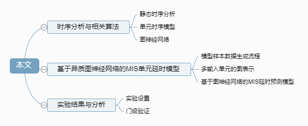
Timing modeling considering multi-input switching effects
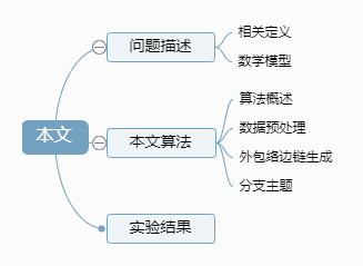
A fast copper pouring algorithm for circular features on high-density printed circuit boards
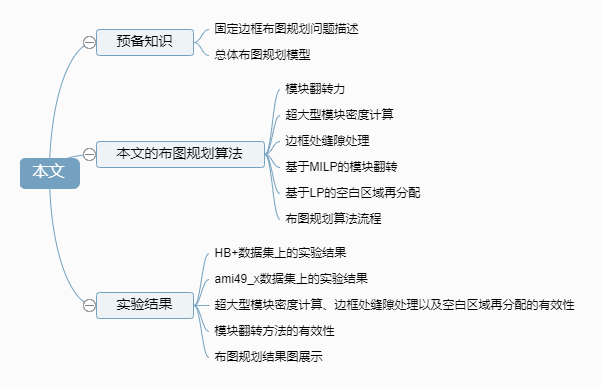
A fixed-frame layout planning based on electrostatic field considering module flipping and blank area redistribution
Wu Haoying1, Xu Jingxue1, Xu Ning1, Zou Sizhan1, Hu Jianguo2
(1. School of Information Engineering, Wuhan University of Technology, Wuhan 430070; 2. Shenzhen Research Institute, Sun Yat-sen University, Shenzhen 528406)
Abstract: To solve the problems of low routing efficiency and poor routing results of the automated routing algorithm for flexible circuit boards, a flexible circuit board routing planning algorithm based on pattern routing is proposed, which uses pattern routing to approximate the detailed routing, reducing the precision error between detailed routing and routing planning. Meanwhile, four routing patterns and several fan-out patterns are designed based on human experience to simulate the resource allocation inside the fan-out area and the possible arrangements and combinations between fan-out areas. For the layer allocation problem, a layer allocation algorithm is designed based on a comprehensive evaluation of the current routing results and the future impact on other nets, and for the constraint that no holes are allowed in the channel area, a non-crossing sequence of routing net topologies in the channel is obtained based on the order of the fan-out area connection positions, which serves as the arrangement order constraint for the point positions on the dividing line. Finally, by comprehensively comparing the results of each pattern, the result with the lowest cost is selected as the final routing planning result. Testing with multiple industrial cases shows that compared with existing flexible circuit board routing planning algorithms, this routing planning algorithm can improve detailed routing efficiency and routing results.
This paper citation format: Wu Haoying, Xu Jingxue, Xu Ning, et al. A flexible circuit board routing planning algorithm based on pattern routing [J]. Integrated Circuits and Embedded Systems, 2024, 24(1): 25-31.
Ding Wenjie, Jiang Haiyang, Zhang Zhanhua, Cao Peng
(Southeast University National ASIC Engineering Center, Nanjing 210096)
Abstract: With the continuous development of integrated circuit technology, the increase in circuit operating frequency and the exacerbation of process deviations have made the impact of multi-input switching (MIS) effects on static timing analysis increasingly significant, making it difficult for traditional single-input switching (SIS) mode cell timing library methods to avoid violations of hold time and setup time. To characterize the impact of MIS effects in timing analysis, several MIS delay models have been proposed in recent years, but most of these models ignore the influence of input switching time and load on MIS effects, resulting in low accuracy. At the same time, these models model each cell separately, ignoring the relationship between MIS effects and the transistor-level topology of the cells, further affecting characterization accuracy and requiring high characterization costs. This paper proposes a MIS cell delay prediction framework based on heterogeneous graph neural networks, modeling the transistor-level topology circuit of multi-input cells as a heterogeneous graph, effectively characterizing the factors influencing MIS delay comprehensively, and training the MIS effects of multiple input gates into a unified model. Under the 16 nm process, the model has been validated on multiple sets of multi-input cells. Experimental results show that this model reduces the modeling overhead to 8.8% of that required for the ANN model, with an average error of only 1.19% for the cells, achieving a 2.05-fold improvement in accuracy compared to the ANN model.
This paper citation format: Ding Wenjie, Jiang Haiyang, Zhang Zhanhua, et al. Timing modeling considering multi-input switching effects [J]. Integrated Circuits and Embedded Systems, 2024, 24(1): 32-38.
Fang Jingke1, Xu Ning1, Zhang Xuelin1, Sun Xianwei1, Hu Jianguo2
(1. School of Information Engineering, Wuhan University of Technology, Wuhan 430070; 2. Shenzhen Research Institute, Sun Yat-sen University, Shenzhen 518057)
Abstract: With the high integration of printed circuit boards, traditional chip installation and heat dissipation can no longer meet the overall size and weight requirements. Copper pouring, as the final key step in PCB design, plays an important role in improving the performance and effectiveness of the circuit board. This paper proposes a fast copper pouring algorithm based on complete shape information classification and area computation for circular features on high-density printed circuit boards, and presents a search scheme for isolated islands generated during the copper pouring process. The core idea is as follows: first, based on the shape information, a large number of features are divided into areas, then clustered based on collision relationships, obtaining the outer envelope edge chain and island edge chain from the clustering results, and finally obtaining the copper pouring results through the edge chain relationships of rings and holes. The algorithm runs in a Windows 10 environment with 3.20 GHz and 16 GB memory, using industrial case test data for validation. Experimental results show that compared to open-source polygon fitting-based copper pouring tools, when facing large-scale scenarios, the copper pouring results are not dependent on the number of edges of the fitting polygon, and the time is reduced by about 60%.
This paper citation format: Fang Jingke, Xu Ning, Zhang Xuelin, et al. A fast copper pouring algorithm for circular features on high-density printed circuit boards [J]. Integrated Circuits and Embedded Systems, 2024, 24(1): 39-45.
Liu Duanxiang1, Huang Fuxing1, Li Xingquan2, Zhu Wenxing1
(1. Discrete Mathematics and Theoretical Computer Science Research Center, Fuzhou University, Fuzhou 350108; 2. Pengcheng Laboratory, Shenzhen 518000)
Abstract: Currently, layout planning based on analytical methods has achieved good results, and module flipping has practical application scenarios that can further optimize results, but analytical methods cannot handle the module flipping problem. Therefore, this paper attempts for the first time to use a unified analytical method to solve this problem, proposing a new force, namely flipping force. In the overall layout planning phase, the flipping force can flip each module to the ideal direction based on wire length. In addition, a new overall layout planning process is designed based on an electrostatic field model. In this process, special handling of density calculations for ultra-large modules is performed to reduce the repulsive force of ultra-large modules, allowing other modules to be closer to ultra-large modules, thus achieving a more uniform module distribution. To better utilize the blank areas in the gaps at the border, a gap handling method at the border is proposed. Finally, a post-processing phase is added to the layout planning algorithm to further optimize the layout results. This post-processing phase first optimizes the flipping direction of modules based on a mixed-integer linear programming flipping model, and then uses the new blank area redistribution method proposed in this paper. This method reduces the number of constraints in the linear programming problem and allows for multiple rounds of optimization, effectively shortening wire length compared to previous methods. Experimental results on the HB+ and ami49_x benchmark circuits show that the layout planning algorithm proposed in this paper reduces the average half-perimeter wire length by at least 13.3% and 13.7% compared to the best layout planning algorithms.
This paper citation format: Liu Duanxiang, Huang Fuxing, Li Xingquan, et al. Considering module flipping and blank area redistribution based on electrostatic field for fixed frame layout planning [J]. Integrated Circuits and Embedded Systems, 2024, 24(1): 46-57.

Yao Hailong: Professor at the School of Computer and Communication Engineering, University of Science and Technology Beijing, doctoral supervisor, head of the EDA Research Center, and executive director of the EDA Joint Laboratory of University of Science and Technology Beijing and BGI. He currently serves as the director of the Physical Realization Subcommittee of the EDA Open Innovation Cooperation Mechanism, executive member of the CCF Integrated Circuit Design Professional Group, and senior member of the IEEE. He has been engaged in research on integrated circuit EDA methods and key technologies for over 20 years, publishing more than 20 papers in top international journals (IEEE TCAD) and conferences (DAC) in the field of EDA. He has won multiple best paper awards/nominations at international conferences in the field of EDA, the first prize of the Wu Wenjun Artificial Intelligence Science and Technology Award for technological invention in 2022 (first contributor), and has been recognized as a “Humboldt Scholar for Experienced Researchers”. He has presided over multiple projects funded by the National Natural Science Foundation of China (key and general), national key research and development plans and sub-projects in the field of EDA.

Welcome to log in to the official website of this journal (www.jices.cn) to submit articles