 I will conduct an in-depth explanation module by module, including design purposes, parameter selection, layout considerations, system design logic, and provide an analysis of advantages and disadvantages. Below is a detailed analysis of the modules in Tesla’s autonomous driving mainboard, divided into five parts: Design Purpose、Parameter Analysis、Layout Logic、Advantages and Disadvantages and Thoughts.
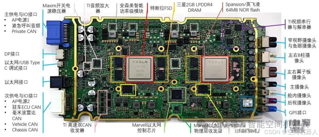
1. Main Power Supply and IO Interface Module
Design Purpose
The main power supply and IO interface module serves to provide stable power input for the entire mainboard while connecting to communication interfaces of other vehicle systems. These interfaces cover core networks of vehicle control such as the CAN bus, emergency call audio functions, etc., aiming to achieve close cooperation between the autonomous driving mainboard and various subsystems of the vehicle.
Parameter Analysis
- AP Power Supply
: Generally derived from the vehicle’s 12V power supply or HV (high voltage) through DC/DC conversion, the mainboard requires stable 3.3V, 5V, and other voltage levels, with current demands depending on specific loads. - Private CAN
: A private CAN network for connecting safety-related or high-priority vehicle subsystems, usually using high-speed CAN (CAN FD) protocol, with bandwidth above 1Mbps, ensuring low latency and high reliability of data. - Emergency Call Audio
: This is the audio channel for the vehicle’s emergency call system, compliant with regulatory requirements, connecting to external communication modules.
Layout Logic
-
Power and IO interfaces are concentrated at the edge of the mainboard for easy connection to the entire vehicle via wiring harness. -
CAN interface area is laid out in a localized manner to reduce signal interference and optimize electromagnetic compatibility (EMC).
Advantages and Disadvantages
Advantages:
-
Compact interface layout with clear wiring. -
Support for multiple communication protocols, adaptable to different vehicle network architectures.Disadvantages: -
High integration level requires strict EMC design; any negligence may introduce signal interference.
Thoughts
This module design reflects the diversity of vehicle network communication interfaces and the importance of power management. The design of the private CAN ensures the independence of safety-related communications, which is a highlight. However, the overly compact layout of this module may affect maintenance and upgrades, especially when the entire vehicle adopts next-generation communication buses (such as Ethernet replacing CAN), which may pose certain adaptation difficulties.
2. DP Interface / Ethernet / USB Type-C Debugging Interface
Design Purpose
These interfaces are primarily used for development, debugging, and high-speed data transmission. USB Type-C is a popular multifunctional interface, while DP (DisplayPort) and Ethernet interfaces serve the display and network communication needs, respectively.
Parameter Analysis
- DP Interface
: Supports 4K or even higher resolution video signal transmission, with bandwidth requirements above 20Gbps. - Ethernet Interface
: Standard 1000BASE-T (Gigabit Ethernet), supporting debugging and data collection. May use TSN (Time-Sensitive Networking) technology to reduce latency. - USB Type-C
: Supports USB 3.1 or higher standards, with transmission rates up to 10Gbps, while being compatible with various power supply needs.
Layout Logic
-
Debugging interfaces are evenly distributed at the edge of the mainboard for easy connection to debugging equipment. -
DP interface is placed close to the image processing module to shorten the signal transmission path and reduce signal integrity (SI) loss.
Advantages and Disadvantages
Advantages:
-
Comprehensive high-speed interface combination meets the high data volume needs of autonomous driving. -
Facilitates debugging and upgrading.Disadvantages: -
High bandwidth requirements increase PCB design difficulty, especially in controlling impedance during high-speed signal routing. -
Increases the quantity and complexity of the mainboard interfaces.
Thoughts
The design of the interface module is very comprehensive, supporting debugging, data transmission, and display functions, providing great convenience for development and testing. However, as Ethernet gradually replaces traditional interfaces, some interfaces may be simplified in the future. Additionally, the multifunctionality of USB Type-C is very suitable for future expansion needs, but attention should be paid to power supply and communication compatibility issues during design.
3. Maxim Switching Power Supply Regulator
Design Purpose
Responsible for converting the input power supply (usually 12V or HV) into various voltages required by the mainboard, such as 3.3V, 5V, or even lower core voltages (1V or below). Maxim switching power supplies are widely used in automotive electronics due to their efficiency and low heat characteristics.
Parameter Analysis
- Input Voltage Range
: Supports vehicle’s 12V power supply or higher voltage input. - Output Voltage Accuracy
: ±1% to ensure stability of core logic voltage. - Efficiency
: Typically above 90%, reducing heat generation.
Layout Logic
-
Power module is placed close to the main power supply interface to shorten input line lengths and reduce conduction interference. -
In a multi-layer PCB stack, the power area uses large copper foil for heat dissipation, while adding filter capacitors to reduce ripple.
Advantages and Disadvantages
Advantages:
-
High conversion efficiency reduces system power consumption. -
Modular design facilitates expansion or upgrades.Disadvantages: -
If layout and filtering design are improper, power noise may interfere with sensitive signal modules (such as camera interfaces).
Thoughts
The choice of Maxim switching power supply is appropriate and meets the automotive industry’s demand for efficient and stable power. However, special attention should be paid to EMI issues, such as optimizing noise suppression by adding shielding on the PCB and reasonable layout.
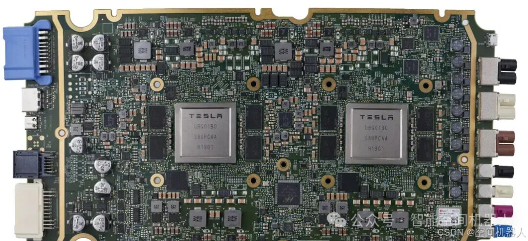
4. Tesla FSD Chip
Design Purpose
This is the core processing unit of the entire mainboard, responsible for all autonomous driving tasks’ calculations, including sensor fusion, environment modeling, path planning, etc. Tesla’s self-developed FSD chip has ultra-high computing power and is optimized for AI tasks.
Parameter Analysis
- Process Technology
: 7nm or below, providing high performance and low power consumption. - Computing Power
: Each chip has a computing power of over 72 TOPS (72 trillion operations per second), supporting deep learning algorithms. - Power Consumption
: Typically within 50W, requiring efficient heat dissipation design.
Layout Logic
-
Two chips are symmetrically placed for easy thermal management and power distribution. -
Storage modules (such as DRAM and Flash) are closely arranged around to reduce latency.
Advantages and Disadvantages
Advantages:
-
Self-developed chips are fully optimized, improving the efficiency of autonomous driving algorithms. -
The dual-chip design provides redundancy, enhancing system reliability. -
Higher power consumption poses significant challenges for heat dissipation and power design. -
Self-developed chip update cycles are long, making it difficult to keep up with the iteration speed of general AI hardware.
Disadvantages:
Thoughts
The FSD chip is Tesla’s leading core advantage, but its design relies too much on self-developed hardware, which may lead to hardware iteration speed lagging behind top AI chip manufacturers (such as NVIDIA). In the future, it may be necessary to find a balance between versatility and performance optimization.
5. Camera Interface Module
Module Function
The camera interface module is the perception core of the autonomous driving system, responsible for receiving and processing image data from cameras around the vehicle. This data is used for object recognition, environmental perception, lane detection, and other core algorithms. The mainboard usually needs to support multiple camera inputs while ensuring high-speed, low-latency transmission.
Design Reasons
- Camera Protocol Support
: Currently, mainstream camera interfaces use MIPI CSI-2 or GMSL (Gigabit Multimedia Serial Link). The MIPI protocol features high speed and low power consumption, suitable for short distances; GMSL is suitable for long-distance, high-speed transmission, so the combination of both can meet different vehicle deployment needs. - Signal Integrity (SI) Requirements
: Due to the large amount of data output by the camera (such as 4K 30fps cameras), the high-speed nature of MIPI and GMSL signals requires strict impedance matching and routing control in the mainboard’s signal integrity design.
Device Parameters
- MIPI Receiver Chip
: For example, TI’s SN65DSI84, supporting 4-channel MIPI input with bandwidth up to 1.5 Gbps/channel. - GMSL Deserializer
: Such as Maxim’s MAX96712, supporting high-speed serial decoding, with power supply reverse function. - Camera Power Consumption Support
: Achieved through PoC (Power over Coaxial), enabling power and data transmission over a single coaxial line, simplifying wiring harnesses.
Layout and System Considerations
- Layout Logic
:
-
MIPI interfaces are placed near the FSD chip to reduce the transmission path of high-speed signals. -
GMSL deserializer is usually placed close to the camera input connector to avoid signal loss caused by long-distance PCB routing.
-
To avoid signal interference, differential pair routing is used in PCB design, and shielding layers are added around the camera interfaces. -
Provide independent power filtering circuits to prevent camera power supply interference with other modules.
Advantages and Disadvantages Analysis
Advantages:
-
Supports multi-protocol input (MIPI + GMSL), adaptable to different in-vehicle scenarios. -
Modular design is easy to expand or maintain.Disadvantages: -
High-speed signal routing requirements are high, which may increase development costs and time. -
Redundancy design is limited (e.g., the number of mainboard interfaces is fixed), making it inflexible to accommodate future increases in camera quantity.
Thoughts
The design of this module takes into account the diversity needs in vehicle deployment, but further optimization of the redundancy design is necessary. For example, the dynamic expansion capability of camera input quantity could be increased, while providing more debugging leeway in signal integrity optimization (such as adding impedance matching adjustment networks).
6. Flash Storage Module
Module Function
Flash storage is used to store the operating programs, machine learning models, and temporary computational results of the FSD chip. Common types of storage include eMMC, UFS, and SPI NOR Flash.
Design Reasons
- Data Reading Speed
: Autonomous driving requires high real-time performance, necessitating high-performance storage devices, such as UFS 3.1, which has a reading speed of up to 2100MB/s, allowing for quick loading of models and image processing tasks. - Reliability and Longevity
: Durable storage chips (such as industrial-grade MLC NAND or higher-level chips) are selected to ensure long-term use of the device under harsh temperature conditions.
Device Parameters
- UFS Storage
: 128GB and above, supporting Gear 4 mode, with bandwidth up to 11.6 Gbps. - NOR Flash
: Mainly used for storing boot firmware (Bootloader), typically around 64MB in capacity, with relatively low read/write speeds but high reliability. - DRAM (Dynamic Random Access Memory)
: For example, LPDDR4x or LPDDR5, with a capacity of 8GB-16GB, meeting the high bandwidth computing requirements of the FSD chip.
Layout and System Considerations
- Layout Logic
:
-
Flash storage is placed close to the FSD chip, reducing signal path length and latency. -
Multi-layer PCB wiring provides independent power and ground planes for each storage chip, avoiding mutual interference.
-
Redundancy design: Multiple Flash interfaces are provided to ensure switching to backups in case of storage chip failure. -
Use ECC (Error Correction Code) technology to improve data storage reliability.
Advantages and Disadvantages Analysis
Advantages:
-
High-speed storage design meets real-time performance needs. -
Reliability design is sufficient to adapt to automotive-grade harsh environments.Disadvantages: -
Storage chip costs are relatively high. -
Storage interface resources occupy considerable space in the system, limiting the number of interfaces for other modules.
Thoughts
The design of the Flash storage module closely aligns with the needs of autonomous driving applications, especially excelling in speed and reliability. However, to reduce costs, consideration could be given to tiered design for storage requirements. For example, transferring some non-real-time data to lower-cost storage chips to achieve better cost-effectiveness.
7. CAN Communication Module
Module Function
The CAN module serves as an important bridge for communication within the vehicle, responsible for data exchange between the autonomous driving system and other vehicle subsystems (such as VCU, BCM, ESP, etc.). Real-time performance and reliability are the core of its design.
Design Reasons
- Real-time Requirements
: The low latency characteristics of the CAN network ensure rapid synchronization of system states. - Automotive Standards
: Supports CAN FD (Flexible Data Rate), meeting high-speed communication needs (bandwidth 8Mbps). - Multi-Network Isolation
: For safety, different CAN networks are designed separately to avoid low-priority tasks interfering with critical tasks.
Device Parameters
- CAN Transceiver
: Such as NXP TJA1044, supporting high-speed CAN and CAN FD protocols, with operating temperature range of -40℃ to 125℃. - Isolation Devices
: Such as ADI’s iCoupler series, with isolation voltage above 2.5kV, ensuring electrical safety. - Termination Resistor
: 120Ω matching to ensure signal integrity.
Layout and System Considerations
- Layout Logic
:
-
CAN transceiver is placed close to the physical connector to minimize signal path. -
Different CAN networks are partitioned on the PCB to reduce mutual interference.
-
Increase filtering circuits to suppress noise interference from the vehicle’s power supply on CAN signals. -
Design redundancy channels to ensure critical communication can still function in the event of a failure.
Advantages and Disadvantages Analysis
Advantages:
-
High reliability, suitable for harsh automotive environments. -
Multi-CAN network isolation design enhances system safety. -
CAN FD hardware costs are higher than traditional CAN. -
Limited bandwidth, unsuitable for future larger data volume needs.
Disadvantages:
Thoughts
Tesla’s partitioned design and isolation measures in the CAN module reflect the high reliability requirements of automotive-grade systems. However, as Ethernet technology gradually replaces traditional CAN networks, future mainboard designs may need to accommodate a hybrid communication architecture of both Ethernet and CAN.