
In recent years, the concept of FPGA has become increasingly prevalent.
For example, Bitcoin mining has seen the use of FPGA-based mining machines. Additionally, Microsoft previously announced that it would use FPGAs “instead of” CPUs in data centers, among other applications.
In fact, FPGA is not unfamiliar to professionals, as it has been widely used for years. However, most people still do not understand it well and have many questions—What exactly is FPGA? Why should it be used? What are the characteristics of FPGA compared to CPUs, GPUs, and ASICs (Application-Specific Integrated Circuits)?…
Today, with this series of questions in mind, let’s together—unveil FPGA.
1. Why Use FPGA?
As is well known, the Moore’s Law for general processors (CPUs) has reached its twilight, while the scale of machine learning and web services is growing exponentially.
People use custom hardware to accelerate common computing tasks; however, the rapidly changing industry requires that this custom hardware be reprogrammable to execute new types of computing tasks.
FPGA is precisely a hardware-reconfigurable architecture. Its full English name is Field Programmable Gate Array.
FPGA has long been used as a low-volume alternative to ASICs, but in recent years it has been deployed on a large scale in data centers by companies like Microsoft and Baidu, to simultaneously provide powerful computing capabilities and sufficient flexibility.
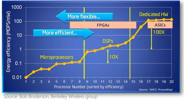
Comparison of performance and flexibility across different architectures
Why is FPGA fast? “It’s all about the company it keeps.”
CPUs and GPUs both belong to the von Neumann architecture, which involves instruction decoding and execution, and shared memory.The reason FPGA has higher efficiency than CPUs and even GPUs is fundamentally due to its architecture, which is instruction-free and does not require shared memory.
In the von Neumann structure, since execution units (like CPU cores) can execute arbitrary instructions, there is a need for instruction memory, decoders, various arithmetic units, and branch jump handling logic. Due to the complexity of control logic for instruction streams, there cannot be too many independent instruction streams. Therefore, GPUs use SIMD (Single Instruction, Multiple Data) to allow multiple execution units to process different data in lockstep, and CPUs also support SIMD instructions.
In contrast, the functionality of each logic unit in FPGA is determined during reprogramming (burning), which means it does not require instructions.
In the von Neumann architecture, memory serves two purposes: one is to maintain state, and the other is for communication between execution units.
Since memory is shared, access arbitration is necessary; to exploit access locality, each execution unit has a private cache, which requires maintaining cache consistency among execution components.
For the need to maintain state, the registers and on-chip memory (BRAM) in FPGA belong to their respective control logic, eliminating unnecessary arbitration and caching.
For communication needs, the connections between each logic unit in FPGA are determined during reprogramming (burning), and do not require shared memory for communication.
Having discussed these high-level concepts, how does FPGA actually perform? Let’s look at both compute-intensive tasks and communication-intensive tasks.
Compute-intensive tasks include matrix operations, image processing, machine learning, compression, asymmetric encryption, and sorting for Bing search, among others. Typically, for these tasks, the CPU offloads the work to the FPGA. For this type of task, the current Altera (which should now be called Intel, but I still prefer to call it Altera…) Stratix V FPGA’s integer multiplication performance is roughly equivalent to that of a 20-core CPU, while its floating-point multiplication performance is comparable to that of an 8-core CPU, but lower by an order of magnitude than that of a GPU. The next-generation FPGA, Stratix 10, which we will soon use, will be equipped with more multipliers and hardware floating-point units, theoretically achieving computing power comparable to that of today’s top GPU computing cards.

Estimated integer multiplication capability of FPGA (not using DSP, estimated based on logic resource utilization)
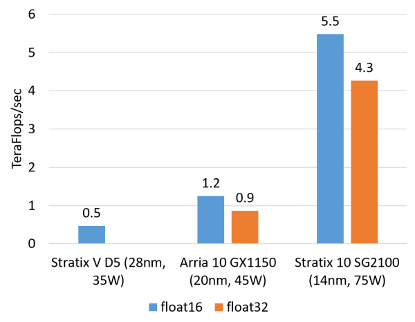
Estimated floating-point multiplication capability of FPGA (float16 using soft core, float32 using hard core)
In data centers, the core advantage of FPGA over GPUs is latency.
For tasks like sorting search results in Bing, it is crucial to return results as quickly as possible, which requires minimizing latency at every step.
If GPUs are used for acceleration, to fully utilize their computing power, the batch size cannot be too small, leading to latencies in the millisecond range.
In contrast, using FPGA for acceleration only requires microsecond-level PCIe latency (our current FPGA is used as a PCIe acceleration card).
In the future, after Intel releases Xeon + FPGA connected via QPI, the latency between CPU and FPGA can be reduced to below 100 nanoseconds, making it comparable to accessing main memory.
Why is FPGA’s latency so much lower than that of GPUs?
This is fundamentally due to architectural differences.
FPGAs possess both pipeline parallelism and data parallelism, while GPUs almost exclusively rely on data parallelism (with limited pipeline depth).
For example, when processing a data packet that involves 10 steps, an FPGA can build a 10-stage pipeline, where different stages process different data packets. Once a packet has passed through all 10 stages, it is processed. As soon as one packet is completed, it can be output immediately.
In contrast, the data-parallel approach of GPUs involves 10 computing units, each processing different packets, but all units must operate in lockstep, doing the same thing (SIMD, Single Instruction Multiple Data). This means that 10 packets must be input and output together, increasing input/output latency.
When tasks arrive one by one rather than in batches, pipeline parallelism can achieve lower latency than data parallelism. Therefore, for streaming computation tasks, FPGAs inherently have a latency advantage over GPUs.
Comparison of the order of magnitude for compute-intensive tasks among CPU, GPU, FPGA, and ASIC (using 16-bit integer multiplication as an example, the numbers are only estimates of orders of magnitude)
ASIC chips are impeccable in terms of throughput, latency, and power consumption, but Microsoft did not adopt them for two reasons:
Data center computing tasks are flexible and variable, while ASIC development costs are high and cycles are long. After deploying a batch of acceleration cards for a certain neural network, if another neural network becomes more popular, the investment would be wasted. FPGAs can update logical functions in just a few hundred milliseconds. The flexibility of FPGAs can protect investments; in fact, Microsoft’s current use of FPGAs is quite different from its initial vision.
Data centers are rented out for use by different tenants. If some machines have neural network acceleration cards, while others have Bing search acceleration cards, and others have network virtualization acceleration cards, scheduling tasks and maintaining the servers would be quite complicated. Using FPGAs can maintain homogeneity in data centers.
Next, let’s look at communication-intensive tasks.
Compared to compute-intensive tasks, communication-intensive tasks are less complex in terms of processing each input data, often just requiring simple calculations to produce output, which can lead to communication becoming a bottleneck. Examples of communication-intensive tasks include symmetric encryption, firewalls, and network virtualization.
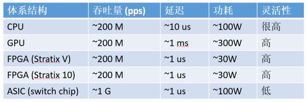
Comparison of the order of magnitude for communication-intensive tasks among CPU, GPU, FPGA, and ASIC (using 64-byte network packet processing as an example, the numbers are only estimates of orders of magnitude)
For communication-intensive tasks, FPGA has even greater advantages over CPUs and GPUs.
In terms of throughput, the transceivers on FPGAs can connect directly to 40 Gbps or even 100 Gbps network cables, processing data packets of any size at line speed; while CPUs must receive packets from network cards before processing, many network cards cannot handle 64-byte small packets at line speed. Although multiple network cards can be inserted to achieve high performance, the number of PCIe slots supported by the CPU and motherboard is often limited, and network cards and switches themselves are quite expensive.
Regarding latency, when packets are received by the CPU from the network card, and then sent back to the network card, even using high-performance packet processing frameworks like DPDK, the latency can still be 4-5 microseconds. A more serious issue is that the latency of general-purpose CPUs is not stable. For example, under high load, forwarding latency can rise to tens of microseconds or even higher (as shown in the figure below); clock interrupts and task scheduling in modern operating systems also add uncertainty to latency.
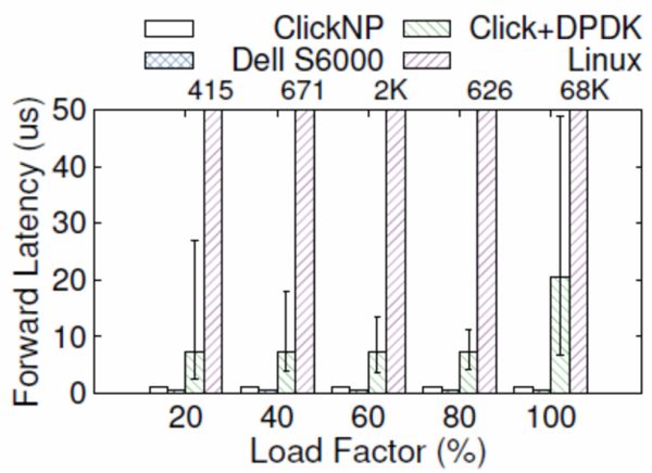
Comparison of forwarding latency between ClickNP (FPGA), Dell S6000 switch (commercial switch chip), Click+DPDK (CPU), and Linux (CPU). The error bar indicates 5% and 95%. Source: [5]
Although GPUs can also handle data packets at high performance, they lack network ports, meaning packets must first be received by the network card before being processed by the GPU. This limits throughput to that of the CPU and/or network card. The latency of GPUs themselves is even worse.
So why not integrate these network functions into the network card or use programmable switches? The flexibility of ASICs remains a hard limitation.
Despite the emergence of increasingly powerful programmable switch chips, such as Tofino that supports P4 language, ASICs still cannot perform complex stateful processing, such as certain custom encryption algorithms.
In summary, the main advantages of FPGA in data centers are stable and extremely low latency, suitable for both streaming compute-intensive tasks and communication-intensive tasks.
2. Microsoft’s Practice of Deploying FPGA
In September 2016, Wired magazine published an article titled “Microsoft Bets Its Future on FPGA,” detailing the history of the Catapult project.
Shortly after, Doug Burger, the head of the Catapult project, demonstrated FPGA-accelerated machine translation alongside Microsoft CEO Satya Nadella at Ignite 2016.
The total computing power of the demonstration was 1.03 million T ops, equivalent to 1.03 Exa-op, comparable to 100,000 top GPU computing cards. A single FPGA (along with on-board memory and network interfaces) consumes about 30 W, only adding one-tenth to the total power consumption of the server.
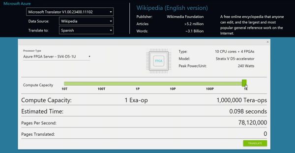
Demonstration at Ignite 2016: Machine translation computing power of 1 Exa-op (10^18) per second
Deploying FPGA at Microsoft has not been a smooth journey. In terms of where to deploy FPGA, there have been three main stages:
Dedicated FPGA clusters filled with FPGAs
One FPGA per machine, using dedicated network connections
One FPGA per machine, placed between network cards and switches, sharing server networks
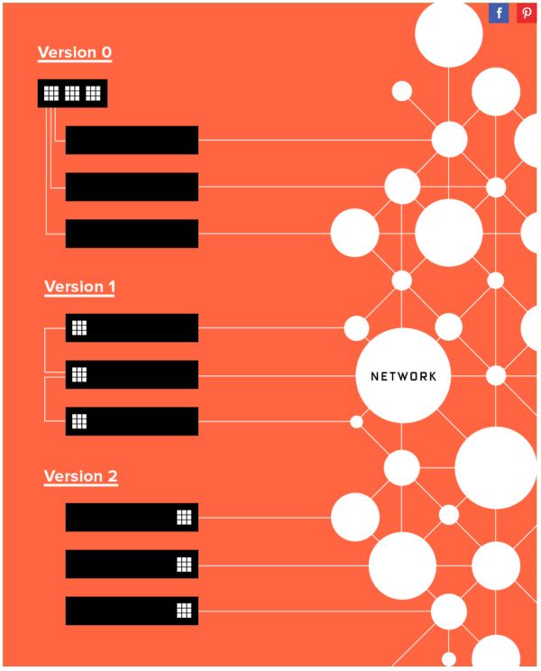
The three stages of Microsoft’s FPGA deployment method, Source: [3]
The first stage involved dedicated clusters filled with FPGA acceleration cards, resembling a supercomputer made entirely of FPGAs.
The image below shows the earliest BFB experimental board, which housed 6 FPGAs on a single PCIe card, with 4 PCIe cards inserted into each 1U server.
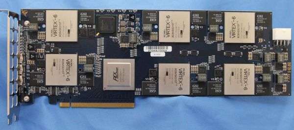
The earliest BFB experimental board, featuring 6 FPGAs. Source: [1]
It is worth noting the name of the company involved. In the semiconductor industry, as long as the scale is large enough, the price of chips tends to approach the price of sand. It is rumored that it was due to this company not agreeing to the “sand price” that another company was chosen.
Of course, both companies’ FPGAs are now used in the data center field. As long as the scale is large enough, concerns over high FPGA prices will become unnecessary.
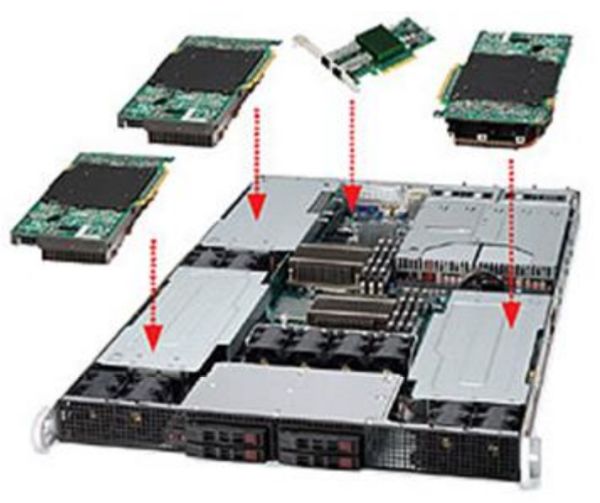
The earliest BFB experimental board, with 4 FPGA cards inserted into a single 1U server. Source: [1]
Deploying FPGAs in a supercomputer-like manner means having an entire cabinet filled with servers like the one shown above, which contains 24 FPGAs (left image).
This approach has several issues:
FPGA communication between different machines is impossible, limiting the scale of problems that FPGAs can handle to the number of FPGAs in a single server;
Other machines in the data center must concentrate tasks to this cabinet, creating in-cast, making it difficult to achieve stable network latency.
Dedicated FPGA cabinets create single points of failure; if one fails, no one can accelerate anything;
Servers with FPGAs are custom-made, complicating cooling and maintenance.
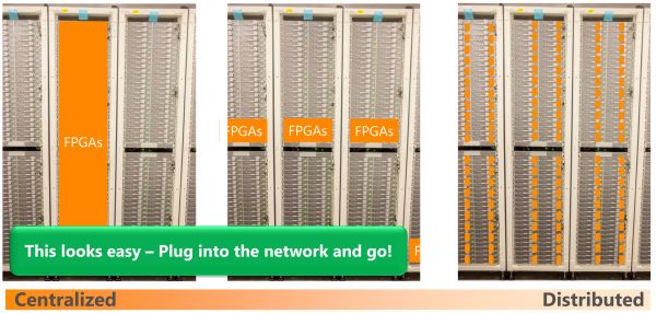
Three methods of deploying FPGAs, from centralized to distributed. Source: [1]
A less radical approach is to deploy a server filled with FPGAs in each cabinet (as shown in the image). This avoids issues (2) and (3) mentioned above, but (1) and (4) remain unresolved.
In the second stage, to ensure homogeneity among servers in the data center (which is also an important reason for not using ASICs), a single FPGA was inserted into each server (right image), with FPGAs connected via dedicated networks. This is also the deployment method published by Microsoft in its ISCA’14 paper.
Open Compute Server in the rack. Source: [1]
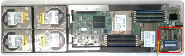
Interior view of Open Compute Server. The red box indicates where the FPGA is placed. Source: [1]
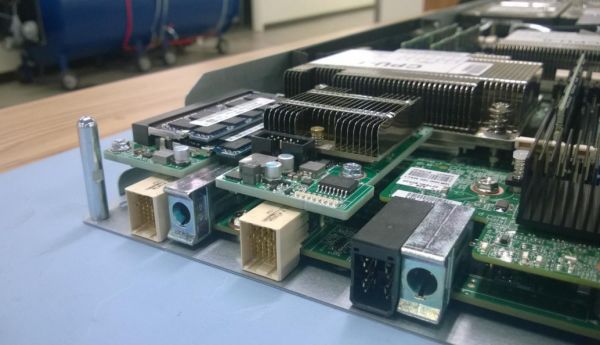
Open Compute Server after inserting FPGA. Source: [1]

Connection and fixation between FPGA and Open Compute Server. Source: [1]
The FPGA uses Stratix V D5, which has 172K ALMs, 2014 M20K on-chip memory, and 1590 DSPs. It has an 8GB DDR3-1333 memory, a PCIe Gen3 x8 interface, and two 10 Gbps network interfaces. The connection between FPGAs in a cabinet employs dedicated networks, with one group of 10G ports connected in a ring of 8, and another group of 10G ports connected in a ring of 6, without using switches.
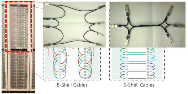
Network connection method between FPGAs in the cabinet. Source: [1]
This cluster of 1632 servers and 1632 FPGAs has improved the overall performance of Bing’s search result sorting by 2 times (in other words, saving half of the servers).
As shown in the image below, every 8 FPGAs form a chain, communicating through the previously mentioned 10 Gbps dedicated network cable. Each of these 8 FPGAs has its role: some are responsible for feature extraction from documents (yellow), some compute feature expressions (green), and some calculate document scores (red).
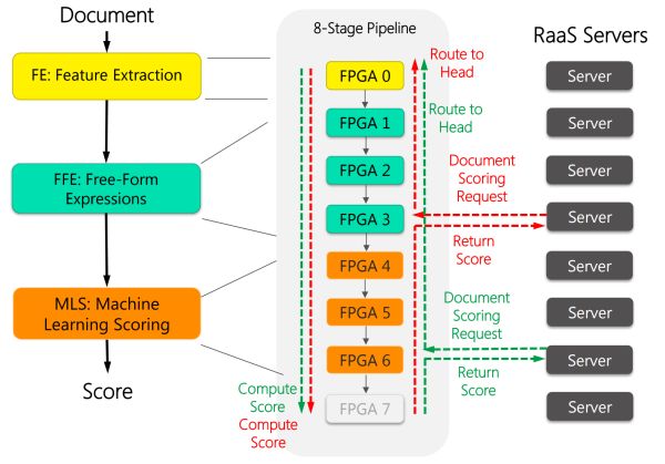
FPGA accelerates the process of Bing’s search sorting. Source: [1]
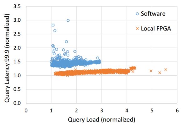
FPGA not only reduces latency in Bing search but also significantly improves latency stability. Source: [4]
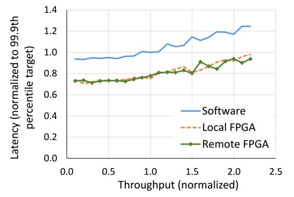
Both local and remote FPGAs can reduce search latency, with the communication latency of remote FPGAs being negligible compared to search latency. Source: [4]
FPGA deployment in Bing has been successful, and the Catapult project continues to expand within the company.
The department with the most servers within Microsoft is the Azure cloud computing department.
The urgent issue faced by the Azure department is the overhead caused by network and storage virtualization. Azure sells virtual machines to customers, needing to provide network functions such as firewalls, load balancing, tunnels, and NAT for those virtual machines. As the physical storage of cloud storage is separated from computing nodes, data must be transported over the network from storage nodes, which also involves compression and encryption.
In the era of 1 Gbps networks and mechanical hard drives, the CPU overhead for network and storage virtualization was negligible. As network speeds reach 40 Gbps and SSDs can achieve throughput of 1 GB/s, CPUs are gradually becoming insufficient.
For example, the Hyper-V virtual switch can only handle around 25 Gbps of traffic, which is unable to achieve 40 Gbps line speed, and performs worse with smaller packets; AES-256 encryption and SHA-1 signatures can only be processed at about 100 MB/s per CPU core, which is only one-tenth of an SSD’s throughput.
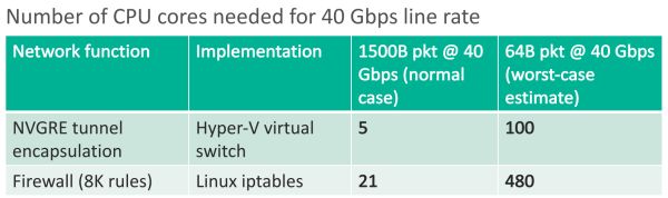
Number of CPU cores required for network tunneling protocols and firewall processing at 40 Gbps. Source: [5]
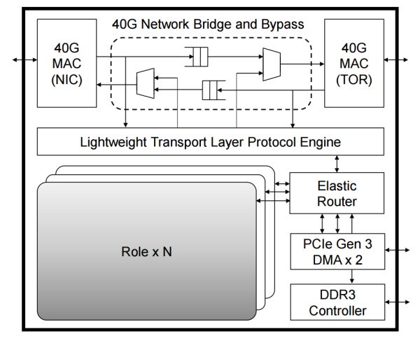
To accelerate network functions and storage virtualization, Microsoft deploys FPGAs between network cards and switches.
As shown in the figure, each FPGA has a 4 GB DDR3-1333 DRAM, connected to a CPU socket through two PCIe Gen3 x8 interfaces (physically a PCIe Gen3 x16 interface, as the FPGA does not have x16 hard cores, logically treated as two x8s). The physical network card (NIC) is just a standard 40 Gbps network card, used solely for communication between the host and the network.
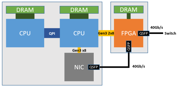
Architecture of Azure servers deploying FPGAs. Source: [6]
FPGAs (SmartNICs) virtualize a network card for each virtual machine, allowing virtual machines to directly access this virtual network card through SR-IOV. The data plane functions that were originally in the virtual switch have been moved to the FPGA, allowing virtual machines to send and receive network packets without involving the CPU or going through the physical network card (NIC). This not only saves CPU resources that can be sold but also improves the network performance of virtual machines (25 Gbps), reducing network latency between virtual machines in the same data center by a factor of 10.
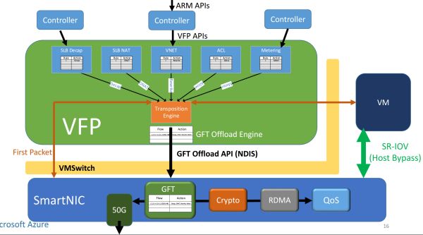
Accelerated architecture for network virtualization. Source: [6]
This is the third-generation architecture for deploying FPGAs at Microsoft, which is also the currently adopted architecture for large-scale deployment of “one FPGA per server”.
The original intention of reusing host networks for FPGAs is to accelerate networking and storage; the more profound impact is that it extends the network connections between FPGAs to a cloud-scale “supercomputer”.
In the second-generation architecture, the network connections between FPGAs were limited to within the same rack, and the dedicated interconnections between FPGAs made scaling difficult, while forwarding through CPUs incurred too high overhead.
In the third-generation architecture, FPGAs communicate through LTL (Lightweight Transport Layer). Latency within the same rack is under 3 microseconds; within 8 microseconds, it can reach 1000 FPGAs; and in 20 microseconds, it can reach all FPGAs in the same data center. Although the second-generation architecture had lower latency within 8 machines, it could only access 48 FPGAs through the network. To support extensive communication between FPGAs, the LTL in the third-generation architecture also supports PFC flow control protocol and DCQCN congestion control protocol.
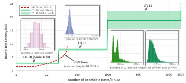
Vertical axis: LTL latency, horizontal axis: number of reachable FPGAs. Source: [4]
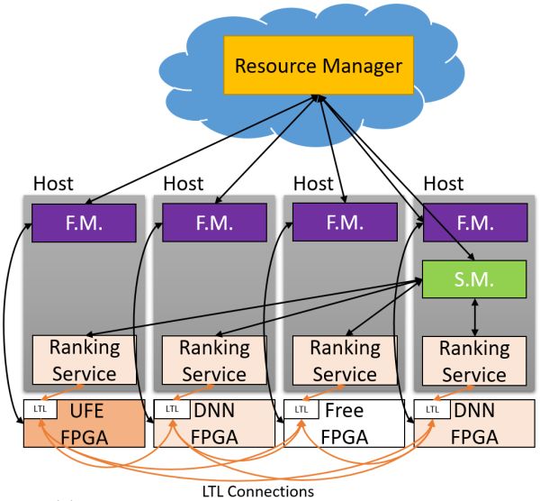
Logical module relationships within FPGA, where each Role represents user logic (such as DNN acceleration, network function acceleration, encryption), while the outer part is responsible for communication between different Roles and between Roles and peripherals. Source: [4]
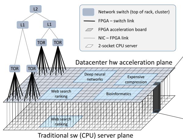
Acceleration plane of the data center formed by FPGAs, positioned between the network switching layer (TOR, L1, L2) and traditional server software (software running on CPU). Source: [4]
The FPGA network, interconnected with high bandwidth and low latency, forms the data center acceleration plane between the network switching layer and traditional server software.
In addition to the acceleration of network and storage virtualization required by every server providing cloud services, the remaining resources on the FPGA can also be used to accelerate tasks like Bing search and deep neural networks (DNN).
For many types of applications, as the scale of distributed FPGA accelerators increases, performance improvements are superlinear.
For instance, in CNN inference, when only using one FPGA, the on-chip memory may not be sufficient to hold the entire model, necessitating constant access to model weights in DRAM, creating a performance bottleneck in DRAM. If the number of FPGAs is sufficient, each FPGA can handle a layer or several features within a layer, allowing the model weights to be fully loaded into on-chip memory, eliminating the DRAM performance bottleneck and fully leveraging the performance of FPGA computing units.
Of course, overly fine segmentation can also lead to increased communication overhead. The key to distributing tasks across a cluster of FPGAs is to balance computation and communication.
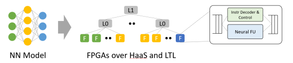
From neural network models to FPGA on HaaS. By leveraging the parallelism within models, different layers and features of the model can be mapped to different FPGAs. Source: [4]
At the MICRO’16 conference, Microsoft proposed the concept of Hardware as a Service (HaaS), which allows hardware to be treated as a schedulable cloud service, facilitating centralized scheduling, management, and large-scale deployment of FPGA services.
Hardware as a Service (HaaS). Source: [4]
From the first generation of dedicated servers filled with FPGAs, to the second generation of clusters with FPGA accelerator cards connected via dedicated networks, to the current large-scale FPGA cloud that reuses data center networks, three guiding principles have shaped our trajectory:
Hardware and software are not in a replacement relationship, but rather a cooperative one;
Flexibility is essential, meaning the ability to be software-defined;
Scalability is a must.
3. The Role of FPGA in Cloud Computing
Finally, I’d like to share my personal thoughts on the role of FPGA in cloud computing. As a third-year PhD student, my research at Microsoft Research Asia aims to answer two questions:
What role should FPGA play in cloud-scale network interconnection systems?
How can we program heterogeneous systems of FPGA + CPU efficiently and scalably?
One of my main regrets regarding the FPGA industry is that the mainstream use of FPGAs in data centers, from internet giants other than Microsoft to the two major FPGA manufacturers and academia, is largely to treat FPGAs as acceleration cards for compute-intensive tasks, similar to GPUs. But is FPGA really suitable for doing what GPUs do?
As previously mentioned, the biggest difference between FPGA and GPU lies in their architectures—FPGAs are better suited for low-latency streaming processing, while GPUs excel in processing large batches of homogeneous data.
Because many people plan to use FPGAs as compute acceleration cards, the two major FPGA manufacturers have also released high-level programming models based on OpenCL, mimicking the batch processing mode of GPUs based on shared memory. When a CPU needs to delegate a task to an FPGA, it must first load the data into the FPGA’s DRAM, then tell the FPGA to start execution, and finally retrieve the results from DRAM.
Why go around through the DRAM on the board when efficient communication could happen directly via PCIe between the CPU and FPGA? Perhaps it is an engineering implementation issue; we find that writing to DRAM, launching a kernel, and reading from DRAM takes about 1.8 milliseconds. In contrast, communication via PCIe DMA only takes 1-2 microseconds.
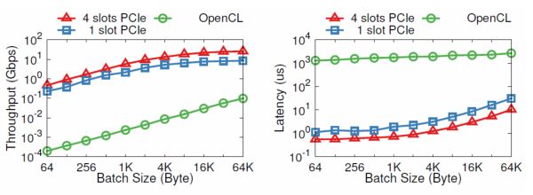
Comparison of PCIe I/O channel and OpenCL performance. The vertical coordinate is on a logarithmic scale. Source: [5]
Communication between multiple kernels within OpenCL is even more exaggerated, as the default method is also through shared memory.
The article opened by stating that FPGA has higher energy efficiency than CPUs and GPUs, fundamentally due to its architecture being instruction-free and not requiring shared memory. Using shared memory for communication between multiple kernels is unnecessary in the case of sequential communication (FIFO). Moreover, DRAM on FPGAs is generally slower than that on GPUs.
Thus, we proposed the ClickNP network programming framework [5], which uses channels for communication between execution units (elements/kernels) and between execution units and host software, instead of shared memory.
Applications that require shared memory can also be implemented based on channels, as CSP (Communicating Sequential Processes) and shared memory are theoretically equivalent. ClickNP is still based on OpenCL, and is limited by the constraints of C language for hardware description (though HLS is indeed much more efficient than Verilog). The ideal hardware description language is probably not C.
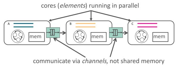
ClickNP uses channels for communication between elements. Source: [5]
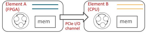
ClickNP uses channels for communication between FPGA and CPU. Source: [5]
Low-latency streaming processing requires the most in terms of communication.
However, due to the limitations of parallelism and operating system scheduling, CPUs are not efficient in communication and their latency is also unstable.
Moreover, communication inherently involves scheduling and arbitration. Because of the limitations of single-core performance and the inefficiency of inter-core communication, the performance of scheduling and arbitration is limited on CPUs, while hardware is well-suited for such repetitive tasks. Thus, my doctoral research defines FPGAs as the “big butler” of communication, capable of accelerating communication between servers, virtual machines, processes, and between CPUs and storage devices.
Success and failure come from the same source. The lack of instructions is both an advantage and a weakness for FPGAs.
Every time something different needs to be done, a certain amount of FPGA logic resources must be allocated. If the tasks are complex and not highly repetitive, they will occupy a large amount of logic resources, most of which will be idle. In this case, it may be better to use a von Neumann structured processor.
Many tasks in data centers exhibit strong locality and repetitiveness: some belong to the network and storage tasks required by virtualization platforms, which are all communication-related; the other part consists of customer computing tasks, such as machine learning, encryption, and decryption.
First use FPGAs for what they do best in communication; perhaps in the future, they will also be rented out as compute acceleration cards like AWS.
Whether for communication, machine learning, or encryption and decryption, algorithms are complex; attempting to completely replace CPUs with FPGAs will inevitably lead to a significant waste of FPGA logic resources and increase development costs for FPGA programs. A more practical approach is to have FPGAs and CPUs work in tandem, with FPGA handling tasks that have strong locality and repetitiveness, while CPUs manage the complex ones.
As we accelerate more and more services like Bing search and deep learning with FPGAs; as the data plane for network and storage virtualization is dominated by FPGAs; as the “data center acceleration plane” formed by FPGAs becomes a significant barrier between networks and servers… there seems to be a feeling that FPGAs will take control, while computational tasks on CPUs may become fragmented, driven by FPGAs. In the past, CPUs were dominant, offloading repetitive computational tasks to FPGAs; will it change to FPGAs being dominant, offloading complex tasks to CPUs in the future? With the advent of Xeon + FPGA, will the old SoC be revitalized in data centers?
“Crossing the memory wall, moving towards a fully programmable world” (Across the memory wall and reach a fully programmable world.)
References:
[1] Large-Scale Reconfigurable Computing in a Microsoft Datacenter https://www.microsoft.com/en-us/research/wp-content/uploads/2014/06/HC26.12.520-Recon-Fabric-Pulnam-Microsoft-Catapult.pdf
[2] A Reconfigurable Fabric for Accelerating Large-Scale Datacenter Services, ISCA’14 https://www.microsoft.com/en-us/research/wp-content/uploads/2016/02/Catapult_ISCA_2014.pdf
[3] Microsoft Has a Whole New Kind of Computer Chip—and It’ll Change Everything
[4] A Cloud-Scale Acceleration Architecture, MICRO’16 https://www.microsoft.com/en-us/research/wp-content/uploads/2016/10/Cloud-Scale-Acceleration-Architecture.pdf
[5] ClickNP: Highly Flexible and High-performance Network Processing with Reconfigurable Hardware – Microsoft Research
[6] Daniel Firestone, SmartNIC: Accelerating Azure’s Network with. FPGAs on OCS servers.
Author Introduction:
Li Bojie, PhD student at the University of Science and Technology of China, Microsoft Research Asia
This article is reproduced with the author’s permission.
Source: Fresh Date Classroom
Editor: tau