Source: SiP and Advanced Packaging Technology
The three main characteristics of Rigid-Flex circuits are Multi-bending, Multi-stackup, and Multi-zone.
In this article, we will take a detailed look at the multi-layered design of Rigid-Flex.
Multi-stackup refers to different numbers of layers and thicknesses in different areas of the substrate, meaning that the substrate requires the definition of multiple stacking structures.
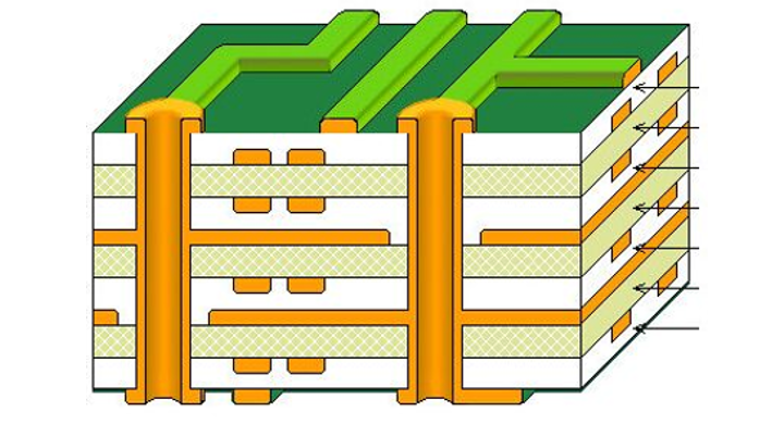
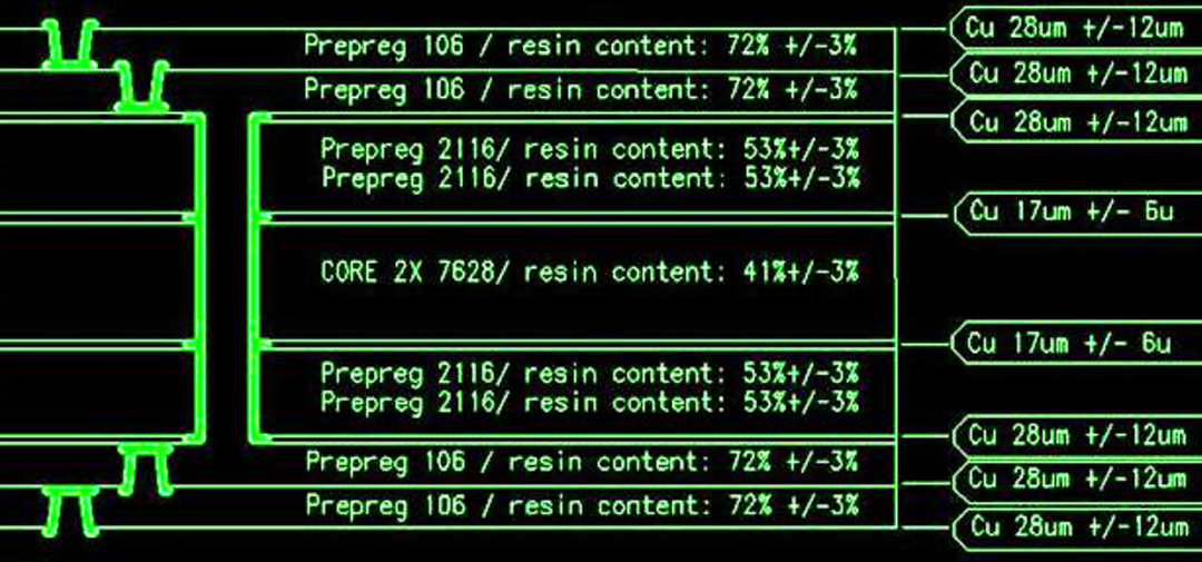
Regardless of the type of substrate, there is at least one stacking structure. For example, commonly seen 4-layer, 6-layer, or 8-layer boards correspond to a specific layer stackup, which we refer to as a single stackup structure. The following image shows the stacking structure of an 8-layer board.
It can be seen that although it is a single stackup structure, the number of layers can still be quite large. Many PCB boards, although they are single stackups, can have dozens or even hundreds of layers. Since the entire board uses a single stacking method, it is called a single stackup structure.
In fact, the demand for stacking varies in different positions of the substrate. Some areas require many layers to increase wiring density and routing efficiency, while others only need a small number of wires. So, can different stacking methods be used in different areas of the board? The answer is yes, which is the idea behind multi-stackup.
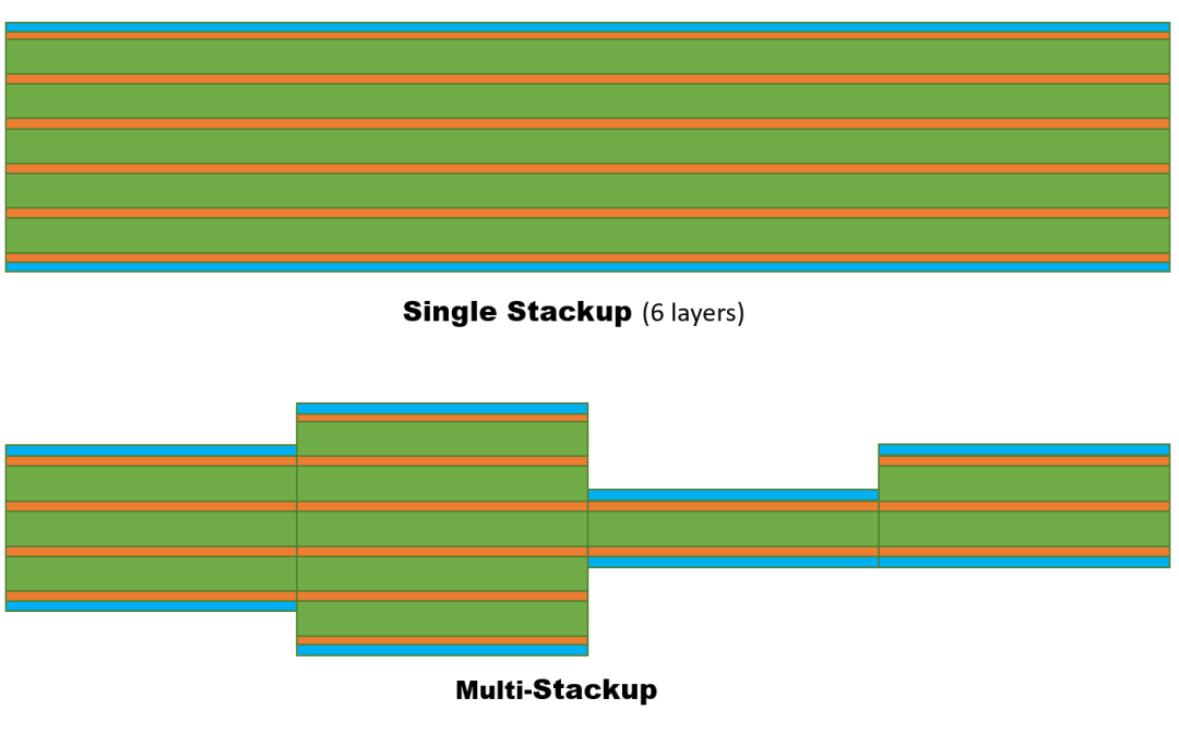
The following image compares single stackup structures and multi-stackup structures:
So, how do we design a multi-stackup structure?
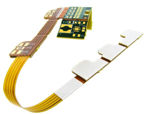
For Rigid-Flex circuit substrates, due to significant functional differences in different areas, some areas need to bend or fold, while others need reinforcement for component installation. A single stackup can no longer meet the requirements, and multiple stacking structures must be used, Multi-stackup.
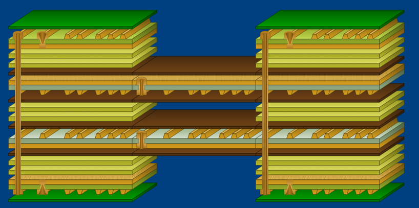
In different positions of the substrate, the thickness and stacking structure vary, as shown in the following image. Thicker stackups are usually applied to rigid substrate parts, while the flexible circuit parts have thinner stackups suitable for bending and folding.
The definition of stacking in Multi-stackup can have dozens of variations. As long as the stacking thickness or materials differ, a new stacking definition is required.
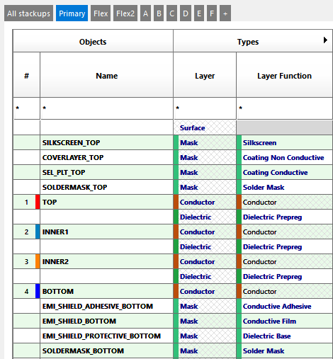
In the image below, we can see that there are already nine stacking definitions: Primary, Flex, Flex2, A, B, C, D, E, F. By clicking on the + sign on the far right, new stackings can be added.
Among all these stacking structures, we can define new stackings or delete existing ones, but there is one stacking that cannot be deleted and always remains in the default position, called the Primary Stackup.
Primary Stackup exists in both multi-stackup and single stackup. Single stackup has only Primary Stackup, while multi-stackup consists of Primary + other Stackups.
In the design software’s Stackup, various stacking structures are defined, and each stacking is assigned corresponding layers, completing the multi-stackup design.
Different Types of Layers
Stackups are composed of different layers, which can be divided into Conductor layers, Dielectric layers, and Mask layers.
The basic feature of multilayer boards is that the Conductor layers and Dielectric layers are placed alternately and then laminated together, connecting the circuits of each layer through vias. The substrate is laminated first and then drilled; this process is called Laminate.
Due to the mechanical drilling used in the laminate method, the hole diameter and spacing are relatively large, making it difficult to meet the demands of high-density designs. As design density increases, laser drilling is adopted, which is more efficient, with smaller hole diameters and higher density. However, lasers can only burn through dielectrics and reflect off metals, so only one layer can be drilled, laminated, and then drilled again, layer by layer, which is referred to as Buildup.
The laminate method uses dielectric materials with high glass fiber content, resulting in higher strength and hardness, while the buildup method uses dielectric materials with high resin content, making it softer and more efficient for laser drilling. In practice, the laminate and buildup methods are often combined, for example, using the laminate method in the middle layers to enhance the board’s strength while employing the buildup method on the outer layers to improve laser drilling efficiency and density.
The image below shows an 8-layer substrate, where the middle four layers use the laminate method, and the outer four layers use the buildup method, creating a 2+4+2 stacking structure.
Outside the top and bottom conductor layers of the substrate, there is usually a Mask layer covering them. For single stack rigid substrates, these Mask layers are usually Soldermask.
For Rigid-Flex circuits, there are various types of Mask layers, typically including: Soldermask, Coverlay, EMI Shielding, Selective Plating, and Stiffener. These Mask layers can be divided into two main categories: conductive Mask and non-conductive Mask.
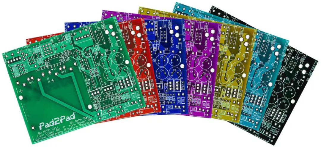
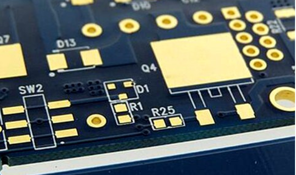
Soldermask is used in both standard rigid substrates and Rigid-Flex circuits. The soldermask used on flexible circuits is a liquid epoxy that cures to a hardened state. Thus, its initial state is liquid, applied to the surface of the substrate through a mask, isolating and protecting the pads. In design, it is usually presented as a negative image, meaning that the areas with patterns are hollowed out, while areas without patterns are filled with epoxy. Soldermask commonly appears green in practical applications, thus also known as “green oil”; however, colors can be flexibly chosen, so other colors of Soldermask are also available.
Currently, a new type of Soldermask known as LPI or LPISM (Liquid Photo Imageable Soldermask) is available. It is a two-component liquid ink that is mixed before application to maintain its shelf life. LPI is superior to epoxy-based liquids, allowing for precise printing and better contact with the PCB, making it more durable.
Coverlay is commonly used in flexible circuits and consists of a polyimide cover layer, serving the same basic function as Soldermask, providing insulation and protection for the outer circuit. Coverlay is presented in a film form, typically as solid polyimide sheets, which differs from the liquid state of Soldermask that cures to a hardened state.
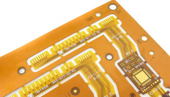
In design, Coverlay is usually applied as a positive design, meaning that the hollow areas are cut out while the patterned areas are covered. Coverlay often appears orange-yellow, covering areas of Rigid-Flex that require insulation and protection.
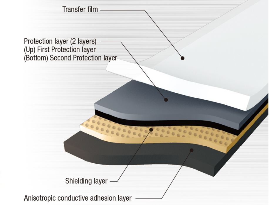
EMI Shielding can shield or reduce the transmission of electromagnetic fields, eliminating unnecessary electromagnetic interference. It prevents signals from entering sensitive systems or prevents signals from leaking out of noisy systems. EMI Shielding can reduce various types of interference, including electromagnetic fields, electrostatic signals, and radio waves.In Rigid-Flex, EMI Shielding is usually applied in the form of large-area conductive films covering the surface of the substrate, forming small metal shapes connected to the top conductor’s GND through openings in the Soldermask or Coverlay.
There is a protective layer above the EMI Shielding and a bonding layer below it for adhesion to the substrate.
Selective Plating involves plating only a portion of the surface of the substrate, rather than the entire surface. This process is commonly referred to as selective plating or brush plating. In some cases, selective plating looks similar to soldering, such as plating on the surface of pads, where the operator holds a flexible brush to apply the plating solution, using the same principle as plating to metallize the pad surface.
In certain areas of flexible circuits, due to the need for soldering components, the strength of the substrate needs to be reinforced. These reinforced parts are called Stiffeners.
Stiffeners usually do not have electrical properties and provide structural reinforcement in specific areas of flexible circuits, supporting devices and connectors structurally.
The above types of layers are commonly used in Rigid-Flex.
Additionally, there are silkscreen layers and solder paste layers, which are also common in rigid substrates, but will not be detailed here.
This content is reproduced and represents only the author’s views
It does not represent the position of the Semiconductor Institute of the Chinese Academy of Sciences
Editor: Wei, a well-known figure