The price differences of mobile phones with varying storage capacities are significant. For those who are frugal, purchasing an external hard drive to regularly transfer phone data and storing the hard drive in the refrigerator is a practical solution. This anecdote highlights the characteristics of external hard drives, such as the need for periodic power and low-temperature storage, as well as data retention time. This article will systematically review the technical principles and characteristics of NAND flash, from the basics to abandonment. 1. NAND Flash Principles – Electronic Cage
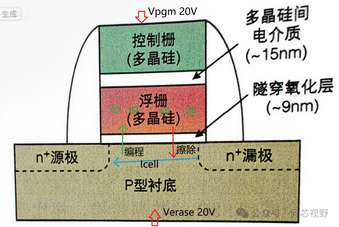 The smallest storage unit of NAND flash is shown in the image above. It achieves the injection (writing) and ejection (erasing) of electrons in the insulated floating gate by controlling the high voltage of the gate and substrate.
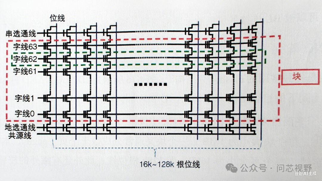 Storage array blocks and pages
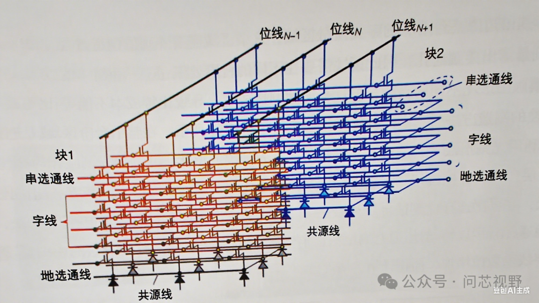 3D NAND array with two blocks as equivalent circuits A storage block shares a substrate and consists of pages, where word lines (WL) connect horizontally to control the gate, and bit lines connect to one end of a string of floating gate transistors. Each string has two select transistors, the top SSL string select and the bottom GSL address select.
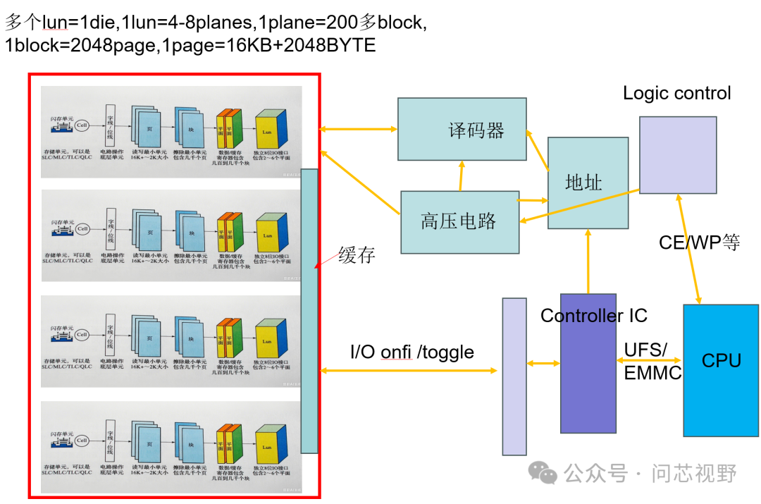 Storage chip block diagram: from page -> block -> plane -> lun -> die -> chip (+controller) The storage system used in electronic products is roughly as shown in the image above, composed of arrays of small storage units. Page: the smallest read unit, block: the smallest erase/write unit, plane: has independent cache decoding circuits, lun: independent logical unit executing commands, die: independent wafer, chip: multiple wafers stacked together, plus the controller, which is what we see as UFS/EMMC chips. The controller chip: also a CPU, helps manage the NAND array, supports SSD/UFS/EMMC interfaces externally, and supports ONFI/toggle interfaces for NAND. The firmware we refer to runs on this, including LDPC ECC modules, bad block management, wear leveling, etc.;2. Read Disturbance – Other Pages in the Same Block To understand read disturbance, one must grasp the reading principle. When reading a page, the selected page needs to apply a voltage VR (VTH_L<VR<VTH_H). If the floating gate has electrons, it will counteract VR, resulting in a very small conduction of the transistor; if the floating gate has no electrons, it will conduct completely. Other transistors in the same column need to apply VpassR≈6V to turn on, and by detecting the drain current Icell, we can determine if the storage is 0 (with electrons) or 1. The problem arises when the unselected transistors are subjected to VpassR, which leads to weak electron injection mode where a small number of electrons are injected into the floating gate. Frequent application of VpassR to MOS transistors may change the number of electrons, ultimately leading to bit flips. Therefore, ECC verification is needed to rewrite, and we validate NAND against read disturbance tests.
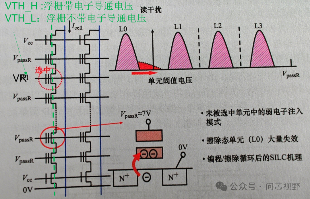 Read disturbance schematic, affected within the same string To avoid the impact of read disturbance, one should use a smaller Vpass voltage whenever possible. Additionally, it is important to record the read count of each block and refresh all data on the block (read, erase, and then write back) before this count reaches a threshold (provided by the flash memory manufacturer), or move the data elsewhere.3. Programming (Write) Disturbance – All Pages in the Same Block are Passively Affected Before programming, the entire block needs to be erased. One must consider why erasure is necessary before programming, and why it must be a full block erase? — AI will provide the answer; writing can only write 0, and when writing 1, if it was originally 0 (with electrons, it must be erased). Full block erasure is necessary because a block shares a substrate. The gate is set to 0V, and 20V is applied to the substrate to pull all electrons away, with string select and address select floating to prevent transistor breakdown.
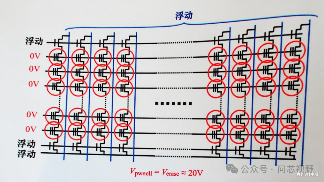 Erase schematic After erasure, there is also an erase verification to check if the erasure is complete,by setting all word lines to 0V, applying VCC to the source line, and then checking the current and voltage of the bit lines (drain). If the current of a certain bit line is 0, then the transistor is off, and this flash memory block should be marked as a bad block.
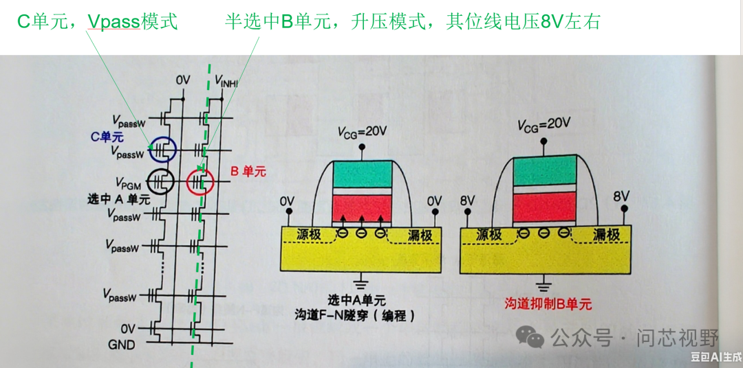 Programming disturbance: the entire block is affected During programming, the selected transistor applies VPGM to inject electrons, and thus the B cells in the same page are also subjected to this voltage. To suppress this voltage, 8V is applied at the source and drain to counteract it. To enable this 8V voltage, VpassW must be applied to all word lines in the same block; this leads to VpassW disturbance in cell C and half-selected disturbance in cell B, affecting the entire block due to the influence of one cell, resulting in passive interference for all. There is also the influence of parasitic coupling capacitance between cells. To avoid the tunneling oxide layer being subjected to maximum electric field during programming, a programming voltage scheme called ISPP (incremental step pulse programming) is used. If interested, you can ask AI; the general idea is to use a lower programming voltage for fast programming state cells and a higher programming voltage for slow programming state cells.
4. Wear Leveling
Floating gate transistors are sensitive to the insulating layer (Tunnel oxide) beneath the floating gate. The thickness of this oxide layer decreases (due to continuous process scaling) or degrades (Degradation, due to many erase/write cycles), significantly affecting the charge within the floating gate. As the erase/write cycles increase, the oxide layer of the floating gate transistor gradually degrades, creating numerous charge traps that consume electrons. This leads to a reduction in the number of electrons entering the floating gate after writing. The wear level of a flash memory block is measured by the number of erase/write cycles (PEC). As the number of erase/write cycles increases, the reliability of the data in the floating gate decreases. When the number of erroneous data exceeds the error correction capability of the controller, the flash memory becomes unusable. To address wear issues, SSD firmware typically employs wear leveling algorithms to evenly distribute writes across all flash memory blocks, preventing certain blocks from being frequently erased and leading to premature failure due to excessive bad blocks.
5. Data Retention
Data is stored in transistors, with the floating gate surrounded by insulators. However, over time, the electrons stored in the floating gate can “escape” through the insulator under the influence of the intrinsic electric field. Especially as the tunneling oxide layer’s isolation effect gradually weakens (with increased erase/write cycles), it becomes easier for electrons to “escape”. When the number of escaping electrons reaches a certain level, a bit “0” may flip to a bit “1”. If the number of bit flips exceeds the error correction capability of the controller (or if NAND is powered off), user data may be lost. The duration of data retention is not only related to the number of erase/write cycles (the more cycles, the shorter the retention period) but also to temperature: the higher the temperature, the faster the data loss. Electronic products need to be charged and powered on regularly, not only to protect the battery but also to protect the storage.
6. Firmware
Firmware is the most important software algorithm after the performance of the chip itself. Many of the NAND characteristics mentioned earlier, in the context of scaling down the chip to increase capacity, rely heavily on firmware to ensure data remains accurate over time. Power loss protection, LDPC, wear leveling, garbage collection, write protection, buffer management, bad block management, logging, and upgrades are all implemented by firmware. Moreover, different application scenarios have varying requirements for NAND specifications; some prioritize read/write speed, while others focus on data reliability, all of which can be achieved through targeted firmware.
7. Key Parameters
tPROG: Program page operation time (single page programming time);
tR: Read page operation time (single page read time);
tBERS: Block erase time (full block erase time);
P/E C: Erase/write cycles;
Sequential read/write (MB/S), random read/write (K IOPS);
Power consumption: active/idle/sleep;
8. NAND Industry:
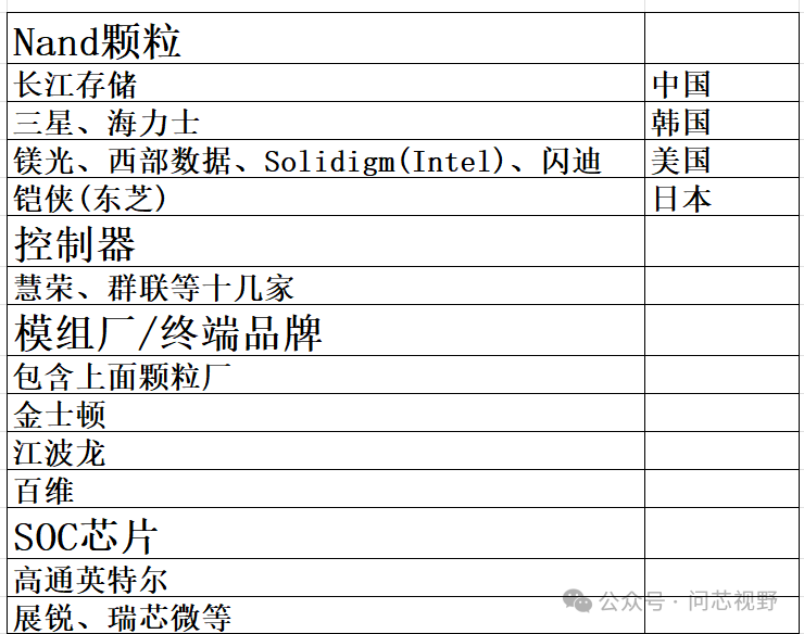
References: Images in the text are sourced from: “Semiconductor Memory Devices and Circuits” by Yu Shidong, “NAND Flash Technology” by You Liucheng
The previous article briefly mentioned NAND flash, and there may be fewer updates on NAND in the future;
Some key concepts of NAND flash