
Modeling of Parasitic Capacitance in Planar Transformers
and Optimization of PCB Windings

Planar transformers can reduce the size of magnetic components and improve the power density of converters, and they have been widely used in electric vehicles, server power supplies, energy storage, and other fields. However, in practical applications, planar transformers face significant parasitic capacitance issues due to reduced inter-turn distances and increased layer overlap, leading to soft-switching loss and EMI problems. Therefore, modeling and suppressing parasitic capacitance is an urgent issue to be addressed.
Research shows that the voltage distribution between windings affects the magnitude of parasitic capacitance. The parasitic capacitance in PCB windings is numerically equivalent to a parallel distribution without altering the original series configuration of the inductive windings. Thus, addressing the voltage distribution across the windings is key to studying parasitic capacitance issues. To tackle the aforementioned challenges, the research team proposed a “symmetric winding arrangement” to filter winding losses, conducting in-depth analysis on six optimized winding structures and proposing two methods, “winding exchange” and “capacitance substitution,” to reduce parasitic capacitance. The optimized winding structure reduces both winding losses and parasitic capacitance.
Related results were recently published in the internationally renowned journal IEEE Transactions on Industry Applications.
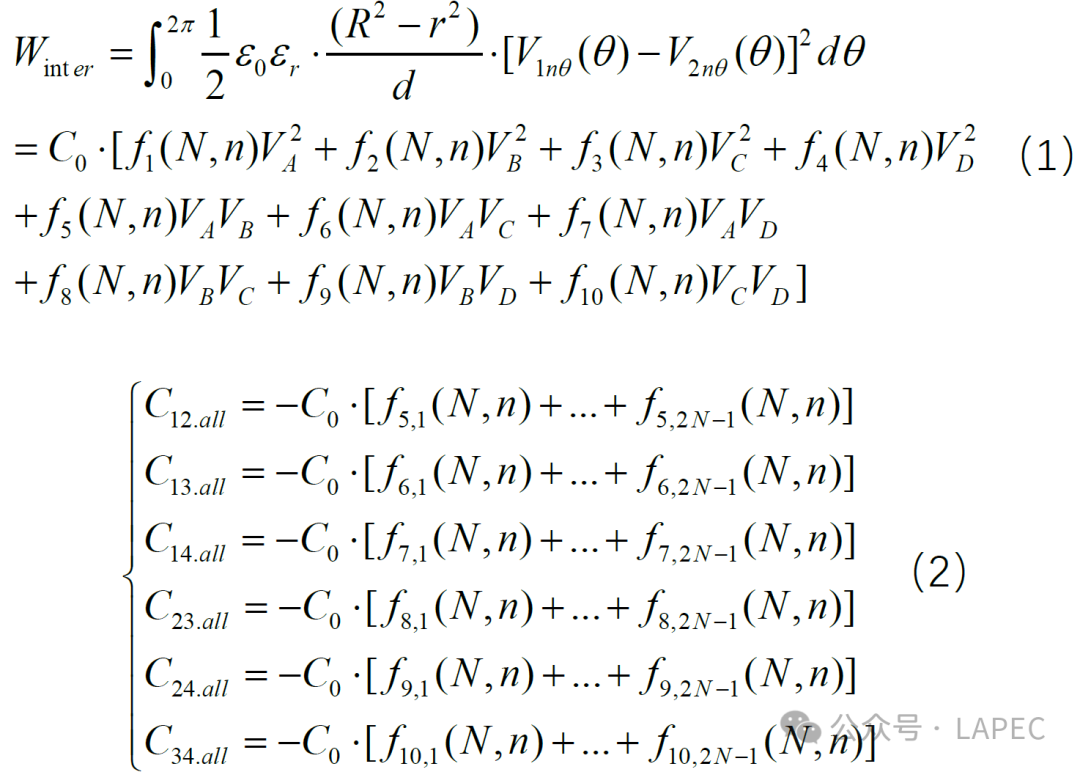
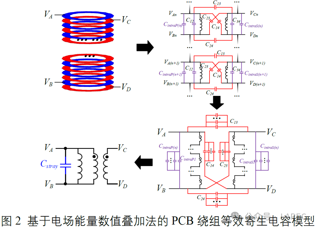
The capacitance calculation for multilayer winding transformers can be extended from single-layer windings. For the single-layer model shown in Figure 1, the stored electric field energy between the windings can be calculated as expressed in Equation (1), and its integral result can be represented as a polynomial expression of the winding port voltages. Similarly, for transformers with multiple windings, each single-layer model divided according to the winding interleaving principle can also yield similar polynomial expressions as in Equation (1). According to the scalar superposition principle of energy, the energy coefficients between each pair of windings can be summed, and the total energy expression can be simplified to the form of Equation (2). Furthermore, based on the definition of the six-capacitance model, the equivalent capacitance at the external terminals of the transformer can be calculated. The equivalence process is illustrated in Figure 2.

The derivation of the parasitic capacitance model for multi-turn transformers is fundamentally based on the principle that the multi-turn model can be viewed as the superposition of several two-turn models. The electric field energy expression for each two-turn model is a function of the winding port voltages. Since the voltage along the winding is linearly distributed in the direction of the current, the port voltage in each two-turn model satisfies a linear relationship with the transformer port voltage. Therefore, the parasitic capacitance calculated for each two-turn model can be linearly equivalent to the corresponding voltage port, and the superposition of these models yields the multi-turn parasitic capacitance model. According to the characteristics of capacitors in parallel, the parasitic capacitance model of the PCB windings can be considered as maintaining the original series relationship of the inductance formed by the windings, while the parasitic capacitance formed between the windings is viewed as an “equivalent parallel” relationship.
For the analysis of winding losses, this paper proposes a winding symmetry arrangement optimization method based on the Dowell theorem, which involves winding a certain number of primary windings adjacent to an equal number of secondary windings, ensuring that the overall magnetic potential of the windings returns to 0. The distribution of AC winding losses after arrangement is shown in Figure 3, and the six arrangements with relatively low losses are selected to further apply the capacitance modeling method for capacitance calculations.
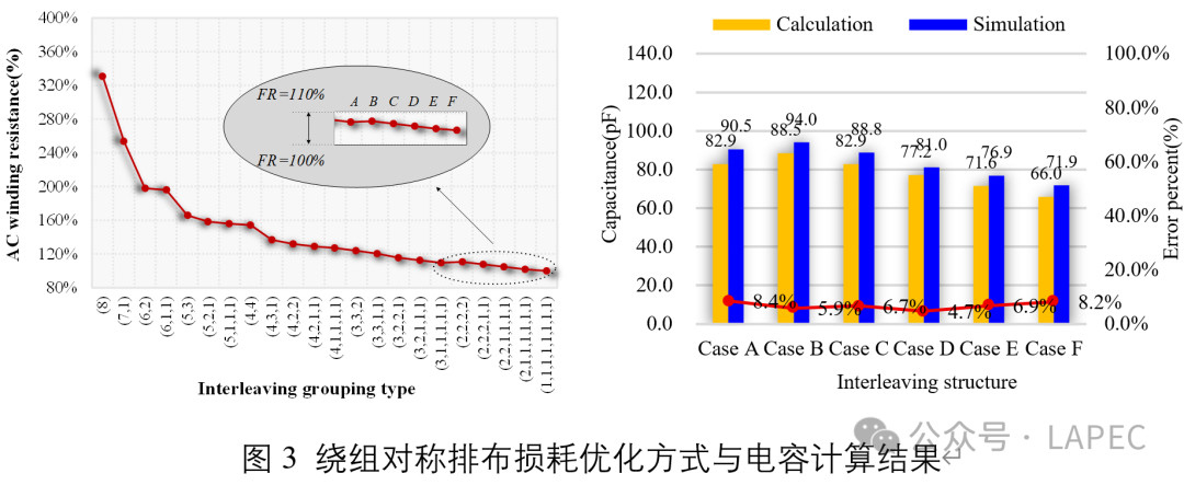
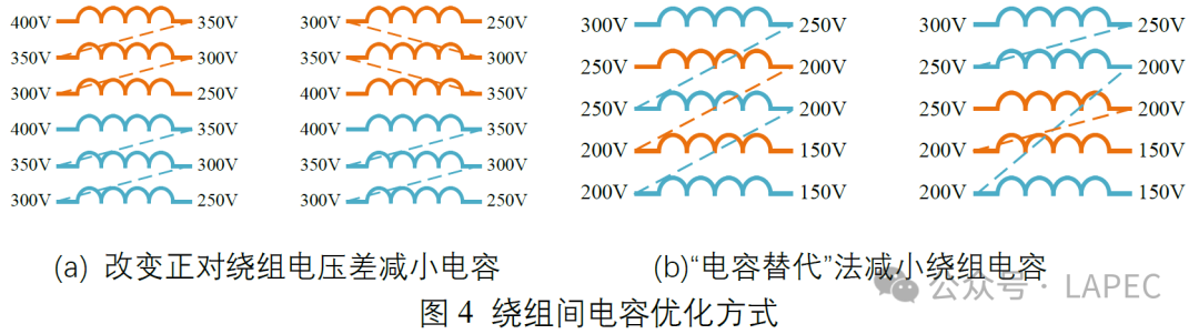
It is worth considering that, under general assumptions, we believe that increasing the degree of interleaving of the windings will lead to an increase in capacitance. According to this theory, among the six arrangements, the one with the deepest interleaving, Case A, should have the smallest capacitance, while the one with the shallowest interleaving, Case F, should have the largest capacitance. However, this contradicts the simulation and calculation results. The reason is that the interleaving of primary and secondary windings only reduces the capacitance within the windings but increases the capacitance between the windings. If the energy increase due to the increased inter-winding capacitance is less than the decrease in the intra-winding capacitance, it can lead to a situation where interleaving not only does not increase capacitance but actually reduces it, as seen in Case F having a capacitance value smaller than Case A. Therefore, when adjusting the winding arrangement to reduce capacitance, it is necessary to consider the trends of both intra-winding and inter-winding capacitance changes. Thus, we identify two methods to reduce parasitic capacitance: one is to adjust the winding arrangement order to reduce the voltage difference across the opposing windings, and the other is to utilize the structural characteristics of PCB to consider the “replacement” of different types of capacitors to achieve a reduction in equivalent capacitance.
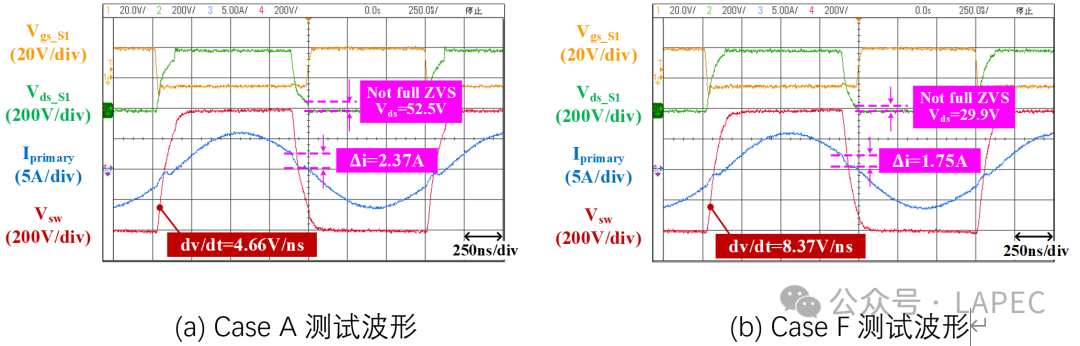
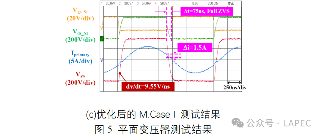
Experimental tests of the CLLC resonant converter under full load conditions are shown in Figure 5. M.Case E achieved complete ZVS, with the switch turning on when the drain-source voltage drops to zero, indicating that the dead time setting under this structure is optimal, allowing for efficient energy transfer and minimal switching losses. In contrast, under the same dead time settings, Case A and Case F did not achieve complete ZVS, with the drain-source voltages at switching moments being 52.5 V and 29.9 V, respectively, indicating that both had higher switching losses than M.Case E. Reducing parasitic capacitance can significantly lower the decline of the magnetizing inductance current during dead time, and this effect is also reflected in the decrease of the primary current at the start of the dead time: M.Case E only decreased by 1.5 A, while Case A and Case F decreased by 2.37 A and 1.75 A, respectively. Furthermore, the rate of change of the primary voltage in M.Case E is significantly higher, being 2.04 times that of Case A and 1.14 times that of Case F, further reducing switching losses. Since all test conditions were consistent except for the transformer windings, the increase in dv/dt at the winding terminals can be attributed to its smaller parasitic capacitance.
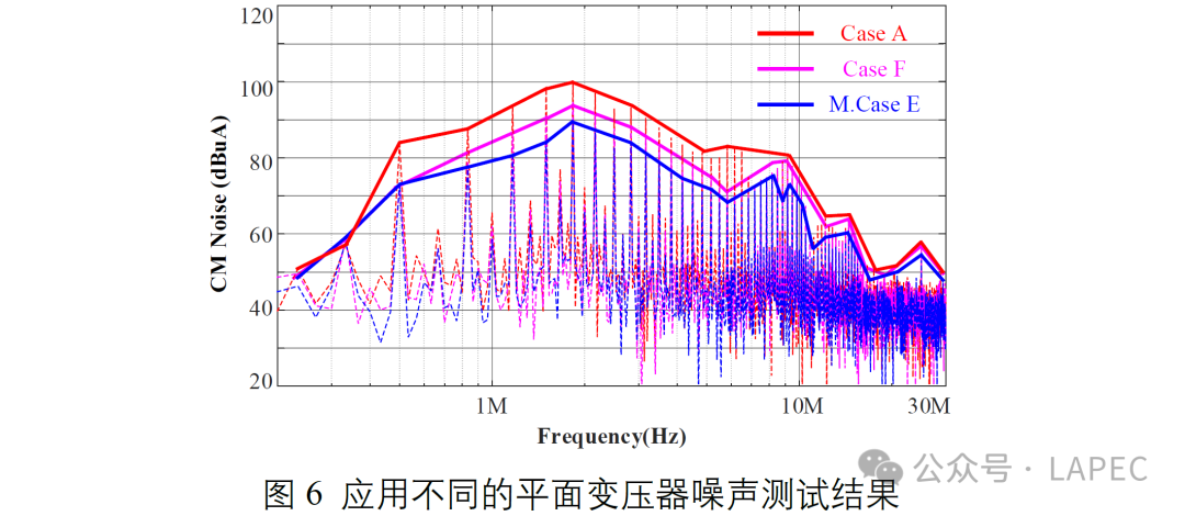
By measuring the common-mode current flowing through the Y capacitance between the primary and secondary grounds, common-mode noise was tested for three winding structures. Figure 6 presents the spectral comparison results of the measured common-mode current after Fourier analysis. The comparison indicates that within the EMI conduction frequency range from 150 kHz to 30 MHz, the optimized M.Case E structure exhibits lower noise than the other two structures, with a corresponding spectral reduction exceeding 6 dBµA.
The above research represents the team’s beneficial exploration in the optimization design of planar transformer PCB windings, achieving further optimization of PCB winding design under loss optimization conditions, demonstrating the feasibility and effectiveness of the capacitance calculation method and the parasitic capacitance suppression method for PCB windings, providing new ideas for the design of high-performance planar transformers.

Hang Wang, Shaoliang An, Xiangdong Sun, Yue Liu and Hongfei Wu, “Optimized PCB Winding with Reduced Parasitic Capacitance for Bidirectional CLLC Resonant Converter,” IEEE Transactions on Industry Applications, doi: 10.1109/TIA.2025.3601575.