Cortex-A78, X1, Mali-G78 Released! ARM’s Three Musketeers Explained
Click the above Computer Enthusiasts to follow us
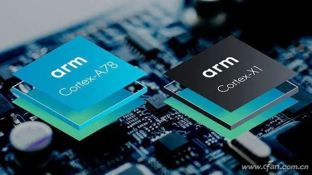
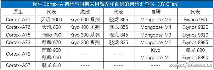
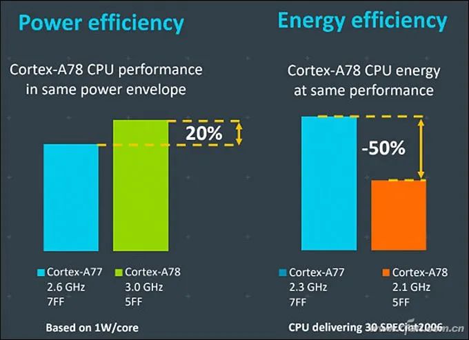
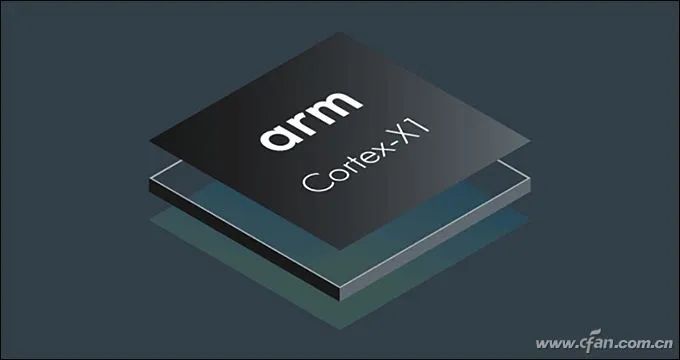
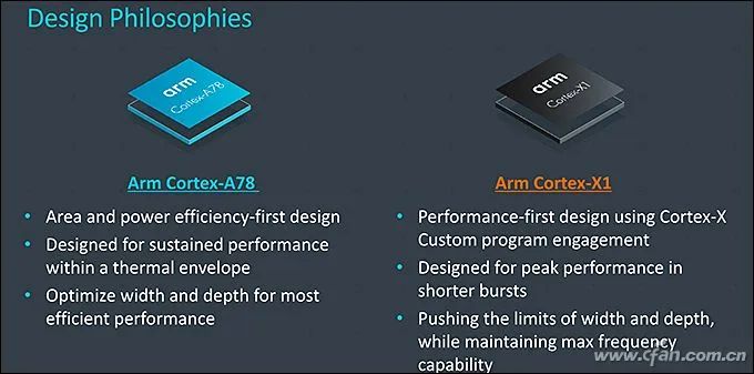
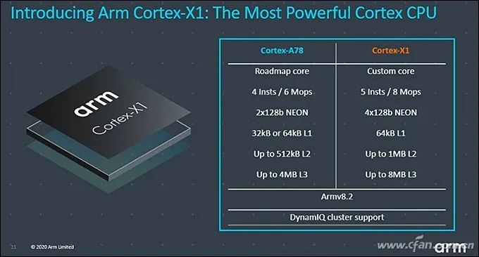
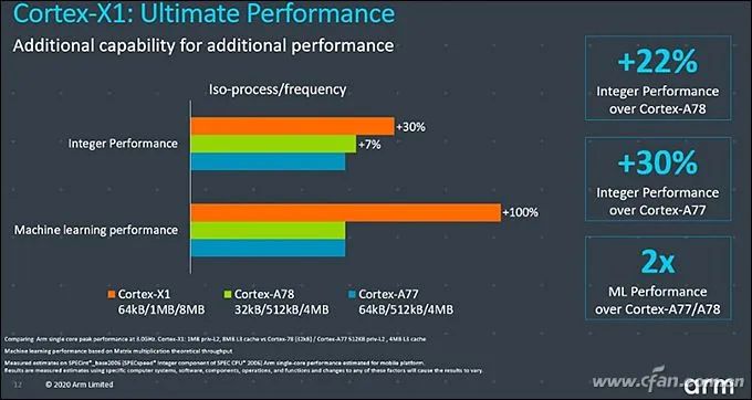
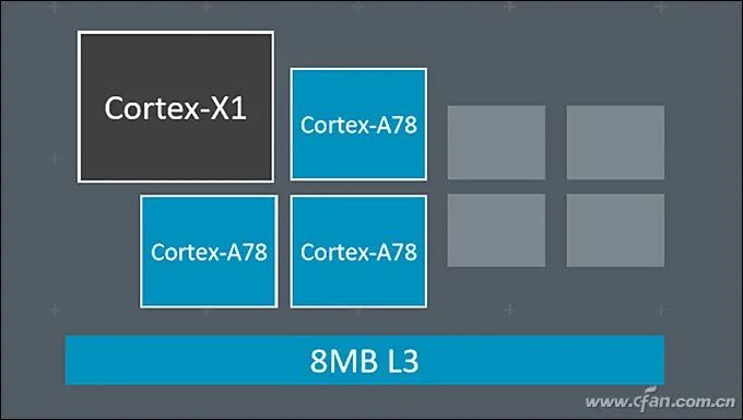
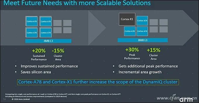
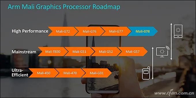
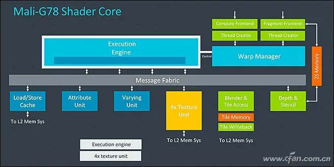
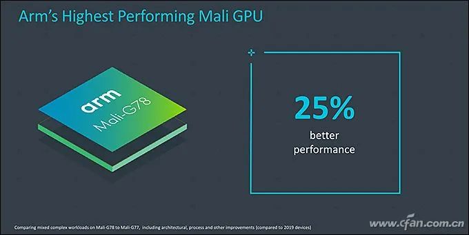
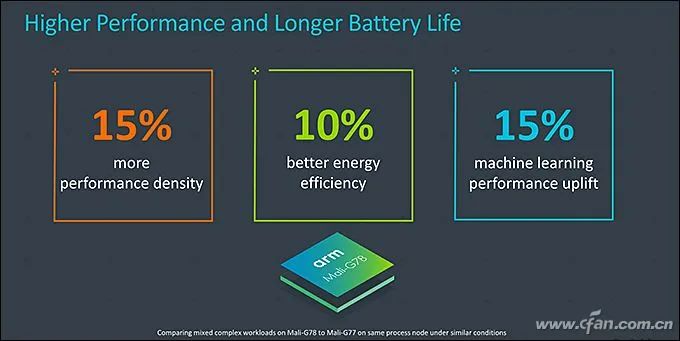
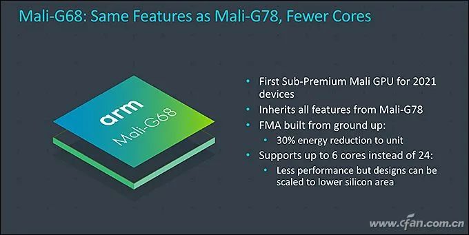
In May 2019, ARM released the Cortex-A77 CPU and Mali-G77 GPU architecture (more accurately, IP, also known as core licensing), and the recently mass-produced Dimensity 1000+ is the first flagship 5G SoC to adopt the above IP combination.Last night, ARM officially released the next-generation IP, consisting of the “Three Musketeers”: Cortex-X1, Cortex-A78, and Mali-G78. Starting with the Kirin 1000, which will be released this September, future 5G SoCs will benefit from them and are expected to further narrow the performance gap with the concurrent Apple A-series SoCs.So, what are the features of ARM’s new generation of “Three Musketeers”?Related Articles:Why is Snapdragon 865 the Most Powerful? Understanding CPU and GPU Architectures!Hardcore Science! Why is SoC performance dependent on architecture and process?The Biggest Regret of Kirin 990! What’s So Good About ARM Cortex-A77 Architecture?Self-research is the way out! See how Qualcomm and Samsung fiercely counter Apple A11 processorWhy can iPhones always outperform others? This is Apple’s proud capital!Cortex-A78: Regular Iteration UpdateCurrently, 5G SoCs like Snapdragon 865, Dimensity 1000, and Exynos 980 all use the Cortex-A77 architecture as the “big core” in their CPUs, thus gaining powerful computing power.As the successor to Cortex-A77, Cortex-A78 does not have any essential changes. Cortex-A76, A77, and A78 all share the same Austin microarchitecture, and there are many commonalities in the design of the three generations of cores.According to ARM, this means that chip suppliers (like Qualcomm, MediaTek, etc.) can easily upgrade their SoC’s IP design without spending too much effort and cost, thus shortening the development cycle.Therefore, do not have too high expectations for Cortex-A78’s performance. ARM’s official data shows that A78 only improves IPC (architecture performance) by 7% compared to A77, with a 4% reduction in power consumption, a 5% reduction in core size, and a 15% reduction in the area of the quad-core cluster.Fortunately, paired with Cortex-A78 is the latest 5nm process technology, which inherently has a better energy efficiency ratio.Currently, a single “big core” in the SoC consumes about 1W at full load. At this time, the Cortex-A77 produced with a 7nm process can run at 2.6GHz, while the Cortex-A78 produced with a 5nm process can reach 3GHz, which means a 20% performance gain at the same power consumption.On the other hand, at the same performance level, the 2.1GHz Cortex-A78 produced with a 5nm process consumes 50% less power than the 2.3GHz Cortex-A77 produced with a 7nm process, which helps improve the battery life of 5G phones.To be honest, ARM’s calculation method is quite confusing, unreasonable, and unfair. If Cortex-A77 were also produced with a 5nm process, its performance would improve significantly compared to the 7nm process, and power consumption would also drop significantly.Conversely, if Cortex-A78 were produced with a 7nm process, its performance and power consumption would not necessarily be much better than Cortex-A77.However, the combination of new processes and new architectures is the trend of technological development and the most economical, which is also beneficial for marketing. So let’s not dwell on it too much.Cortex-X1: The End of Self-ResearchSince the iPhone 5, Apple’s A-series processors have embarked on a “self-research” journey, which is why each generation of iPhones can almost lead all processors in the Android phone circle.所谓的“自研”,就是购买ARM最高级的指令集授权,然后根据自身需要开发兼容ARM的架构,能领先ARM公版的Cortex-A架构多少全看芯片商的技术水平。Qualcomm once adopted a self-researched Krait architecture during the Snapdragon 600/800 era, and the latest Snapdragon 820 is also self-researched Kyro. However, Qualcomm found that the energy efficiency of self-researched architectures is difficult to lead significantly over the public Cortex-A architecture, which is not economical. Therefore, starting from Snapdragon 835, they adopted the BoC strategy, which is what we commonly refer to as “magic modification”, customizing based on the existing public Cortex-A architecture.Since the Kirin 980, Huawei has also adopted a similar approach, basing its big cores on the Cortex-A architecture, which is also a form of magic modification. It is important to note that the public Cortex-A architecture has very few areas that can be “magic modified”. Most manufacturers basically only cut into the cache part, so whether it’s Qualcomm or Kirin, the performance difference between their modified cores and the public architecture is not significant; the key still lies in the frequency.Samsung joined the self-research army starting from Exynos 8890 and launched a core architecture called Mongoose. However, after four generations of self-research, Samsung decided to abandon the self-researched Mongoose core at the end of 2019 and disbanded the entire R&D team located in Austin, Texas, and will fully use ARM’s design solutions in the future.It can be seen that, except for Apple, the self-research path of other chip manufacturers is fraught with difficulties and thankless.The good news is that the Cortex-X1 released by ARM as part of the “Three Musketeers” is actually a type of IP core that allows chip manufacturers to perform extensive customization on it, completely replacing the arduous “self-research” path.From the architectural details disclosed by ARM, both Cortex-X1 and Cortex-A78 operate under the ARMv8.2 instruction set, which is compatible, but Cortex-X1 is a custom CPU core. The decoding bandwidth has been increased from 4 lanes to 5 lanes, an increase of 25%, and the NEON floating point has been increased from 2 lanes of 128b to 4 lanes of 128b, effectively doubling the floating point performance. In terms of cache, Cortex-X1 can have an L1 cache of up to 64KB, an L2 cache of 1MB, and an L3 cache of up to 8MB, which is double that of Cortex-A78.Based on the improvements mentioned above, Cortex-X1 can achieve a 30% increase in single-core performance and a 100% increase in AI performance compared to the previous generation A77.According to ARM’s plan, in the future, Cortex-X1 will serve as the “super big core” within flagship 5G SoCs, while Cortex-A78 will be considered a regular “big core”, together with Cortex-A55 to form a “1+3+4” tri-cluster DynamIQ cluster, achieving a perfect balance between performance and power consumption.The only regret is that the Cortex-X1 core will occupy a larger package area. ARM’s data shows that 4 Cortex-A78 cores paired with 4MB L3 cache can achieve a 20% performance improvement over the previous generation A77, while the core area is reduced by 15%; whereas 1 Cortex-X1 + 3 Cortex-A78 cores with 8MB L3 cache will see a 15% increase in core area, but peak performance will increase by 30%.In other words, Cortex-X1 can bring at least an additional 10% performance improvement over Cortex-A78, which doesn’t seem like much, right?Mali-G78: Dramatic Increase in Compute UnitsIn the Android field, ARM’s public version of the Mali series GPUs has already dominated, and the old rival PowerVR has been marginalized. The advent of the new generation Mali-G78 GPU will further consolidate ARM’s leading position in the GPU field.Perhaps due to the lack of significant competitive pressure, Mali-G78 continues to use the Valhall graphics architecture adopted by Mali-G77, but it has optimized the global clock domain, changing it to a new two-level structure, which separates the upper shared GPU module from the actual shader core frequency, creating an asynchronous clock domain. This allows the GPU core to operate at different frequencies from other parts, which can be fast or slow, thus solving the imbalance between geometric output and computation, textures, and engine, while also allowing the GPU to operate at different voltages, thereby reducing power consumption and improving energy efficiency, which is a common practice in desktop-level CPUs and GPUs.In addition, Mali-G78 also completely rewrote the FMA (fused multiply-add) engine, including a new multiplication architecture, a new addition architecture, and FP32/FP16 floating points, which can save 30% in power consumption.During the Mali-G77 era, it could be equipped with a maximum of 16 compute units, i.e., Mali-G77 MC16, but due to cost, heat generation, and power consumption constraints, even the most aggressive Exynos 990 only used 11 compute units, i.e., Mali-G77 MC11, while Dimensity 1000+ was equipped with Mali-G77 MC9.This time, Mali-G78 can be armed with up to 24 compute units, a 50% increase over its predecessor. However, as mentioned above, even with the latest 5nm process, the actual commercial maximum scale is estimated to be around 16, as more would lead to overheating issues in phones.According to ARM’s data, thanks to improvements in architecture, process, and other aspects, the performance of Mali-G78 can be improved by up to 25% compared to Mali-G77, even under the same process conditions, it can improve by 15%, while energy efficiency can improve by 10%, and machine learning performance can increase by 15%.It looks pretty good.Moreover, ARM has also introduced the Mali-G68 GPU to fill the gap between the Mali-G7 series and Mali-G5 series. From the existing data, the architecture and parameters of Mali-G68 are identical to those of Mali-G78, but it can only be equipped with a maximum of 6 compute units.In other words, a Mali-G78 equipped with 1 to 6 compute units is called Mali-G68, while one with more than 6 compute units is called Mali-G77.The Kirin 1000 series, which will be released in September, is expected to be the first to feature the Cortex-A78 and Mali-G78 5G SoC, but whether it will use the Cortex-X1 architecture remains to be seen. Next year’s Snapdragon 875, Dimensity 2000, and Exynos 1000 series will also use at least one member of the “Three Musketeers”; as for how much their actual performance will improve compared to existing flagships, we shall wait and see.
Click “Read the Original” for more exciting content