Source:This article is compiled by Semiconductor Industry Observer (ID: icbank) from AnandTech
Recently, Apple launched their brand new MacBook series products. This is not an ordinary release; if there is anything different, it is that what Apple did today is something that has not happened in 15 years: the beginning of a CPU architecture transformation for the entire consumer Mac series.
This tremendous change is thanks to the company’s vertical integration in hardware and software, and no one but Apple could introduce it so quickly. The last time Apple attempted something like this was in 2006 when they abandoned IBM’s PowerPC ISA and processors in favor of Intel’s x86 design. Now, Intel is being discarded as Apple adopts internally designed processors and CPU microarchitectures based on Arm-ISA.
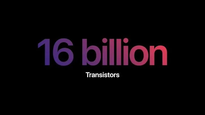
The new processor is called Apple M1, which is the company’s first SoC designed for Macs. It features four high-performance cores, four efficiency cores, and an 8-core GPU, with 16 billion transistors built on a 5nm process node. Apple is launching a new SoC naming scheme for this new processor series, but at least in theory, it looks very much like the A14X.
The event included many new official announcements, but also lacked (in typical Apple fashion) detailed information. Today, we will dissect the new Apple M1 news and conduct an in-depth study of the microarchitecture based on the already released Apple A14 SoC.
Apple M1 SoC: A14X for Mac
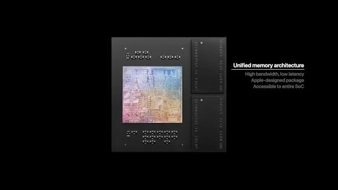
The new Apple M1 indeed marks the beginning of a significant new journey for Apple. In the company’s presentation, they did not reveal much about the design details, but one slide told us a lot about the chip’s packaging and architecture:
This packaging method, which embeds DRAM in organic packaging, is not new for Apple; they have been using it since the A12. When it comes to high-end chips, Apple prefers this packaging over the usual smartphone POP packaging (package on package) because these chips are designed with higher TDP in mind. Therefore, placing DRAM beside the computer chip rather than on top of it helps ensure these chips remain effectively cooled.
This also means we can almost certainly expect to see a 128-bit DRAM bus on the new chip, very similar to the previous generation a-X chips.
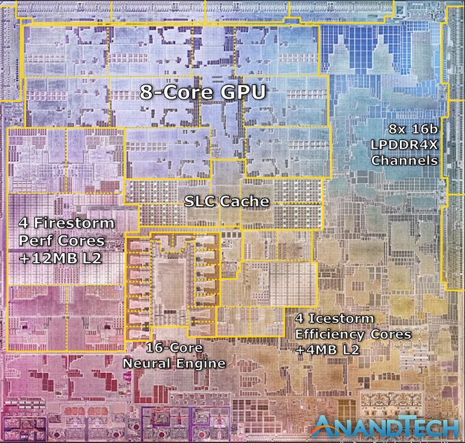
On the same slide, Apple also seemed to use an actual die shot of the new M1 chip. It fully conforms to the chip characteristics described by Apple and looks like a real die photo. This might be the fastest die annotation I’ve ever done:
We can see M1’s four Firestorm high-performance CPU cores on the left. Note the large amount of cache—12MB cache was a surprising discovery at this event, as the A14 still only has 8MB of L2 cache. The new cache appears to be divided into three larger blocks, which makes sense considering Apple’s new configuration transitions from 8MB to 12MB, especially since it is now being used by 4 cores instead of 2.
Meanwhile, four Icestorm efficiency cores were found near the center of the SoC, above which we can find the system-level cache of the SoC that is shared among all IP blocks.
Finally, the 8-core GPU occupies a significant amount of die space and is located in the upper half of this die shot.
The most interesting aspect of the M1 is its comparison with Intel and AMD’s other CPU designs. All the modules mentioned above still cover only a portion of the entire die and come with a large amount of auxiliary IP. Apple mentioned that the M1 is a true SoC, integrating functionalities that previously required several discrete chips inside Mac notebooks, such as I/O controllers and Apple’s SSD and security controllers.
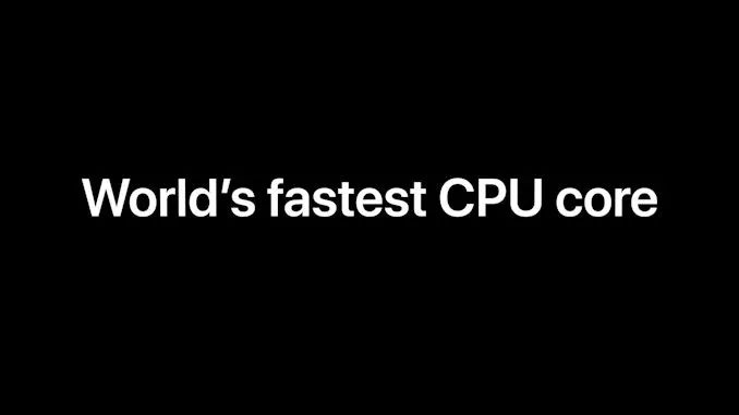
Apple claims it has the world’s fastest CPU cores. This will be the central topic of today’s article as we will delve into the microarchitecture of the Firestorm core and examine performance data from the very similar Apple A14 SoC. Given its additional cache, we expect the Firestorm core used in the M1 to be faster than what we will analyze today with the A14, thus making Apple’s claim of having the fastest CPU cores in the world seem very reasonable.
The entire SoC incorporates 16 billion transistors, which is 35% more than the latest A14 built into the iPhone. If Apple can maintain a similar transistor density between the two chips, we should expect a transistor size of about 120mm. This will be significantly smaller than the previous generation Intel chips in Apple’s MacBook.
In fact, it is a small miracle that Apple could so seamlessly complete a major architectural transition, considering the company’s considerable experience in achieving this. After all, this is not Apple’s first time switching CPU architectures for their Macs.
Around the mid-21st century, the long-standing PowerPC company reached a crossroads, where the Apple-IBM-Motorola (AIM) alliance responsible for PowerPC development found it increasingly difficult to further develop chips. IBM’s PowerPC970 (G5) chip had considerable performance metrics on desktops, but its power consumption was quite significant. This made it unsuitable for the growing laptop market, while Apple was still using Motorola’s PowerPC 7400 series (G4) chips, which, although having better power efficiency, could not compete with Intel’s Core series processors.
Thus, Apple played a card they had kept: the Marklar project. Leveraging the flexibility of Mac OS X and its underlying Darwin kernel (designed to be portable like other Unix systems), Apple maintained an x86 version of Mac OS X. Although initially viewed primarily as a good coding practice exercise, it ensured that the operating system code written by Apple did not have unnecessary constraints tied to PowerPC and its big-endian memory model—Marklar became Apple’s strategy for exiting the stagnant PowerPC ecosystem. The company would switch to x86 processors, particularly Intel’s x86 processors, disrupting its software ecosystem while opening doors for better performance and new customer opportunities.
By all accounts, the switch to x86 was a significant victory for Apple. The performance per watt offered by Intel’s processors far surpassed that of the PowerPC processors Apple left behind, especially after Intel firmly established its dominance in the PC processor space with the launch of the Core 2 (Conroe) series processors at the end of 2006. Ultimately, this laid the groundwork for Apple’s trajectory in the coming years, making them a laptop company with ultra-portables (MacBook Air) and the incredible MacBook Pro. Likewise, x86 compatibility with Windows introduced the capability to boot Windows directly or run it in a virtual machine with very little overhead.
 However, the cost of this transition came from the software side. Developers needed to start using Apple’s latest toolchain to generate universal binaries that could run on both PPC and x86 Macs, and not all of Apple’s previous APIs would carry over to x86. Of course, developers also made leaps, but this was a transformation without any real precedent.
At least to some extent, the gap was narrowed by Rosetta, which was Apple’s PowerPC translation layer for x86. Rosetta allowed most PPC Mac OS X applications to run on x86 Macs, although performance suffered somewhat (running PPC on x86 is not the simplest task), but the higher performance of Intel CPUs helped carry it for most non-intensive applications. Ultimately, Rosetta was just a band-aid for Apple, and they quickly ripped it off; by the time Mac OS X 10.7 (Lion) was released in 2011, Apple had already abandoned Rosetta. Thus, even with Rosetta, Apple made it clear to developers that if they wanted to continue selling and satisfying users, they hoped they would update their applications for x86.
Ultimately, the transition from PowerPC to x86 set the tone for a modern, agile Apple. Since then, Apple has created a whole set of rapidly evolving concepts and changed things wherever they deemed fit, with only limited consideration for backward compatibility. This left users and developers with little choice but to enjoy the ride and keep up with Apple’s trends. But it also gave Apple the ability to roll out new technologies early, breaking old applications if necessary, so that new features wouldn’t be hindered by backward compatibility issues.
All of this has happened before, and all of this will happen again next week when Apple releases its first Macs based on the Apple M1. Universal binaries are back, Rosetta is back, and Apple is urging developers to launch and run their applications on Arm is in full swing. The transition from PPC to x86 created a template for Apple to change ISAs, and after a successful transition, as Apple becomes its own chip supplier, they will do this again in the coming years.
In the following pages, we will examine the Firestorm core of the A14, which will also be used in the M1, and conduct extensive benchmarking on iPhone chips to set the minimum standard for the M1:
However, the cost of this transition came from the software side. Developers needed to start using Apple’s latest toolchain to generate universal binaries that could run on both PPC and x86 Macs, and not all of Apple’s previous APIs would carry over to x86. Of course, developers also made leaps, but this was a transformation without any real precedent.
At least to some extent, the gap was narrowed by Rosetta, which was Apple’s PowerPC translation layer for x86. Rosetta allowed most PPC Mac OS X applications to run on x86 Macs, although performance suffered somewhat (running PPC on x86 is not the simplest task), but the higher performance of Intel CPUs helped carry it for most non-intensive applications. Ultimately, Rosetta was just a band-aid for Apple, and they quickly ripped it off; by the time Mac OS X 10.7 (Lion) was released in 2011, Apple had already abandoned Rosetta. Thus, even with Rosetta, Apple made it clear to developers that if they wanted to continue selling and satisfying users, they hoped they would update their applications for x86.
Ultimately, the transition from PowerPC to x86 set the tone for a modern, agile Apple. Since then, Apple has created a whole set of rapidly evolving concepts and changed things wherever they deemed fit, with only limited consideration for backward compatibility. This left users and developers with little choice but to enjoy the ride and keep up with Apple’s trends. But it also gave Apple the ability to roll out new technologies early, breaking old applications if necessary, so that new features wouldn’t be hindered by backward compatibility issues.
All of this has happened before, and all of this will happen again next week when Apple releases its first Macs based on the Apple M1. Universal binaries are back, Rosetta is back, and Apple is urging developers to launch and run their applications on Arm is in full swing. The transition from PPC to x86 created a template for Apple to change ISAs, and after a successful transition, as Apple becomes its own chip supplier, they will do this again in the coming years.
In the following pages, we will examine the Firestorm core of the A14, which will also be used in the M1, and conduct extensive benchmarking on iPhone chips to set the minimum standard for the M1:
Apple’s Massive CPU Microarchitecture
So how does Apple intend to compete with AMD and Intel in this market? Readers who have been following Apple’s efforts in silicon technology over the past few years will not be surprised to see the performance that Apple claimed during the event.
The secret lies in Apple’s internal CPU microarchitecture. Apple’s long journey in customizing CPU microarchitecture began with the release of the Apple A6 in the iPhone 5 in 2012. Even then, with its first-generation “Swift” design, the company’s performance data was impressive compared to mobile competitors.
However, it was the Apple A7 SoC and the Cyclone CPU microarchitecture released in the iPhone 5S in 2013 that truly caused a stir in the industry. Apple’s early adoption of the 64-bit Armv8 shocked everyone, as the company was the first in the industry to implement the new instruction set architecture, which they even did more than a year ahead of Arm’s own CPU team, as the Cortex-A57 (Arm’s own 64-bit microarchitecture design) would not be released until the end of 2014.
Apple referred to its “Cyclone” design as a “desktop-class architecture,” which, in retrospect, seems to have provided a clear indication of the company’s direction. Over the next few generations, Apple has rapidly evolved their custom CPU microarchitecture, achieving significant performance improvements with each generation, which we have extensively reported over the past few years:
This year’s A14 chip includes the 8th generation of Apple’s 64-bit microarchitecture family, which began with the A7 and Cyclone design. Over the years, Apple’s design cadence seems to have stabilized around major dual-generation microarchitecture updates, starting with the A7 chipset, with the A9, A11, and A13 significantly increasing design complexity and the width and depth of the microarchitecture.
Given that Apple has not revealed any details, Apple’s CPU remains largely a black box design, and the only public resources on this matter trace back to the LLVM patches from the A7 Cyclone era, which are no longer relevant to today’s designs. While we do not have official means and information to explain how Apple’s CPU works, that does not mean we cannot figure out some aspects of the design. However, based on our own internal testing and third-party micro-benchmarking (with special credit to @Veedrac’s microarchitecture test suite), we can disclose some details about Apple’s design. The following disclosures are based on the behavior of the latest Apple A14 SoC tested in the iPhone 12 Pro:
Apple’s Firestorm CPU Core: Bigger and Better
The latest generation of A14’s large core CPU design is codenamed “Firestorm,” continuing the “Lightning” microarchitecture from last year’s Apple A13. The core discussed today is the new Firestorm core and its lineage, which has been continuously improved over the years, and is a key part of how Apple made a significant leap from Intel x86 designs to their own internal SoCs.
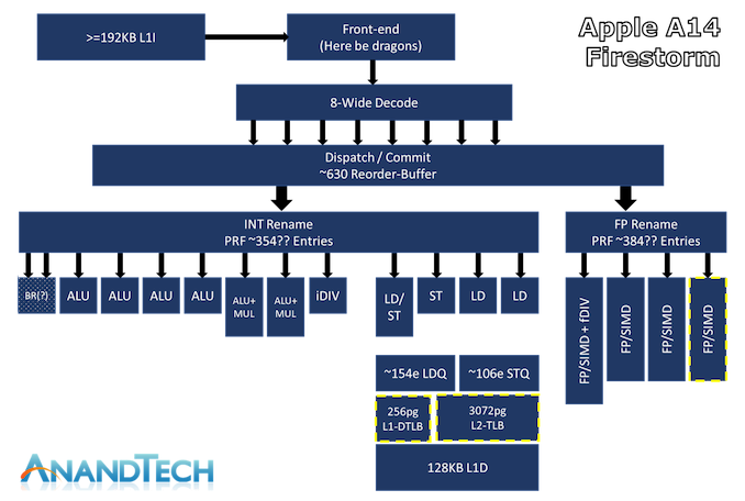
The above diagram is an estimated functional layout of Apple’s latest large core design—here I have done my best to identify the functions of the new design, but still cannot delve exhaustively into all that Apple’s design must provide—thus, there may be some errors.
What truly defines Apple’s Firestorm CPU core compared to other industry designs is the width of its microarchitecture. With an 8-wide decode block, Apple’s Firestorm is currently the widest commercialized design in the industry. The P10 core that IBM is about to launch in POWER10 is the only other design expected to be released on the market with such a wide decoder design, after Samsung canceled their own M6 core, which was also described as having such a wide design.
Today’s other modern designs, such as AMD’s Zen (1 to 3) and Intel’s µarch, x86 CPUs still only use a 4-wide decoder design, which currently seems impossible to scale to a larger range due to the inherent variable instruction length characteristics of the ISA, making it more difficult for designs to manage architecture aspects of the decoder compared to the fixed-length instructions of ARM ISA. On the ARM side, Samsung’s designs have reached 6-wide since the M3, while Arm’s own Cortex cores have steadily expanded with each generation, currently reaching 4-wide in existing silicon and expected to increase to a 5-wide design in the upcoming Cortex-X1 core.
Apple’s microarchitecture being 8-wide is actually not new for the A14. Back to the A13, it seems I made a mistake in testing, as I initially thought it was a 7-wide machine. I recently retested it and confirmed that Apple indeed upgraded it to a 7-wide decode from the A11 and 12 in this generation.
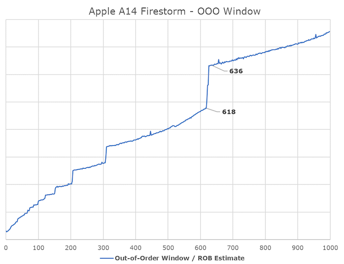 In Apple’s recent designs, one aspect we have never really been able to pinpoint is how deep their out-of-order execution capability is. The last official resource we obtained on this issue was the 192 number for the ROB (Reorder Buffer) in the 2013 Cyclone design. Thanks again to the tests implemented by Veedrac, it seems we can confirm that Firestorm’s ROB is within the range of 630 instructions, which is an upgrade from last year’s A13 Lightning core (measured at 560). It is still unclear whether this is the same as the traditional ROB in other architectures, but the tests at least expose the microarchitecture limits related to ROB and reveal the correct data of other designs in the industry. The out-of-order window refers to the number of instructions the core can “park” and wait to be executed as it attempts to fetch and execute dependencies of each instruction.
For Apple’s new core, an A+-630 deep ROB is a massive out-of-order window, as it far exceeds that of other designs in the industry. Intel’s Sunny Cove and Willow Cove cores are the second largest “deep” OOO designs with 352 ROB entries, while AMD’s latest Zen3 core has 256 entries, and recent ARM designs like Cortex-X1 have 224 entries.
How and why Apple can achieve such disproportionate designs compared to other designers is still unclear, but this seems to be a key feature of Apple’s design philosophy and approach to achieving high instruction-level parallelism.
Having high ILP also means that these instructions need to be executed in parallel by the machine, and here we can also see that Apple’s backend execution engine has a very wide capability. In integers, we estimate its capacity for running instructions and renaming physical register files to be around 354 entries, and we found at least 7 execution ports for actual arithmetic operations. This includes 4 simple arithmetic logic units capable of addition instructions, 2 complex units also having MUL (multiplication) capabilities, and one that seems to be a dedicated integer division unit. The core can handle 2 branches per cycle; I suspect this is achieved by one or two dedicated branch forwarding ports, but I cannot confirm the design layout here 100%.
Here, the Firestorm core seems to have no significant changes in integer design, as the only notable change is that the integer division delay of the unit has noticeably increased (yes).
In floating-point and vector execution, the new Firestorm core is actually more impressive, as Apple has added a fourth execution pipeline, increasing its capability by 33%. Here, the FP renaming register seems to have 384 entries, which is also quite substantial. Thus, these four 128-bit NEON pipelines can theoretically match the current throughput of AMD and Intel’s desktop cores, although they have lower throughput. The endpoint operation throughput here is 1:1 with pipeline count, meaning the Firestorm can execute 4 FADDs and 4 FMULs per cycle, with 3 and 4 cycle latencies respectively. This is four times that of Intel CPUs and previous AMD CPUs, and twice that of the recent Zen3, and of course still operates at lower frequencies. This may be one of the reasons Apple performs so well in browser benchmarks (JavaScript numbers are floating-point double precision numbers).
The vector capabilities of these four pipelines seem to be the same, with the only observed throughput reduction in FP division, reciprocal, and square root operations having only a throughput of 1.
In load/store, we see what seems to be four execution ports: one load/store, one dedicated store, and two dedicated load units. The core can execute up to 3 loads per cycle and up to 2 stores per cycle, but can only execute a maximum of 2 loads and 2 stores simultaneously.
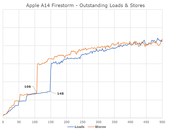
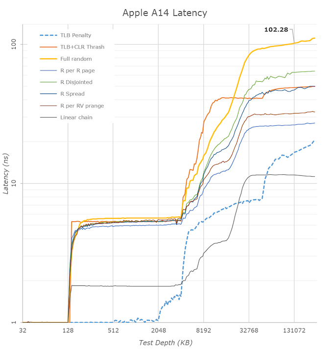
Interestingly, here we see how deep Apple handles memory transactions. We measured around 148-154 outstanding loads and about 106 outstanding stores, which should be equivalent numbers for the load and store queues of the memory subsystem. Unsurprisingly, this is also deeper than any other microarchitecture on the market. By comparison, AMD’s Zen3 and Intel’s Sunny Cove have 128/72 and 128/64 respectively. Intel’s design here is not far off from Apple’s; in fact, the peak throughputs of these latest microarchitectures are relatively matched—if Apple deploys this design to non-mobile memory subsystems and DRAM, it will be very interesting.
The biggest improvement in this generation of Firestorm cores is the TLB. The L1 TLB has doubled from 128 pages to 256 pages, and the L2 TLB has increased from 2048 pages to 3072 pages. This is an absolutely oversized change on today’s iPhones, as the page size is 16KB, meaning the L2 TLB covers 48MB, even exceeding the cache capacity of the A14. As Apple transitions the microarchitecture to Mac systems, compatible with 4KB pages, ensuring the design still provides sufficient performance will be a key part of why Apple chose to make such a large upgrade in this generation.
In Apple’s recent designs, one aspect we have never really been able to pinpoint is how deep their out-of-order execution capability is. The last official resource we obtained on this issue was the 192 number for the ROB (Reorder Buffer) in the 2013 Cyclone design. Thanks again to the tests implemented by Veedrac, it seems we can confirm that Firestorm’s ROB is within the range of 630 instructions, which is an upgrade from last year’s A13 Lightning core (measured at 560). It is still unclear whether this is the same as the traditional ROB in other architectures, but the tests at least expose the microarchitecture limits related to ROB and reveal the correct data of other designs in the industry. The out-of-order window refers to the number of instructions the core can “park” and wait to be executed as it attempts to fetch and execute dependencies of each instruction.
For Apple’s new core, an A+-630 deep ROB is a massive out-of-order window, as it far exceeds that of other designs in the industry. Intel’s Sunny Cove and Willow Cove cores are the second largest “deep” OOO designs with 352 ROB entries, while AMD’s latest Zen3 core has 256 entries, and recent ARM designs like Cortex-X1 have 224 entries.
How and why Apple can achieve such disproportionate designs compared to other designers is still unclear, but this seems to be a key feature of Apple’s design philosophy and approach to achieving high instruction-level parallelism.
Having high ILP also means that these instructions need to be executed in parallel by the machine, and here we can also see that Apple’s backend execution engine has a very wide capability. In integers, we estimate its capacity for running instructions and renaming physical register files to be around 354 entries, and we found at least 7 execution ports for actual arithmetic operations. This includes 4 simple arithmetic logic units capable of addition instructions, 2 complex units also having MUL (multiplication) capabilities, and one that seems to be a dedicated integer division unit. The core can handle 2 branches per cycle; I suspect this is achieved by one or two dedicated branch forwarding ports, but I cannot confirm the design layout here 100%.
Here, the Firestorm core seems to have no significant changes in integer design, as the only notable change is that the integer division delay of the unit has noticeably increased (yes).
In floating-point and vector execution, the new Firestorm core is actually more impressive, as Apple has added a fourth execution pipeline, increasing its capability by 33%. Here, the FP renaming register seems to have 384 entries, which is also quite substantial. Thus, these four 128-bit NEON pipelines can theoretically match the current throughput of AMD and Intel’s desktop cores, although they have lower throughput. The endpoint operation throughput here is 1:1 with pipeline count, meaning the Firestorm can execute 4 FADDs and 4 FMULs per cycle, with 3 and 4 cycle latencies respectively. This is four times that of Intel CPUs and previous AMD CPUs, and twice that of the recent Zen3, and of course still operates at lower frequencies. This may be one of the reasons Apple performs so well in browser benchmarks (JavaScript numbers are floating-point double precision numbers).
The vector capabilities of these four pipelines seem to be the same, with the only observed throughput reduction in FP division, reciprocal, and square root operations having only a throughput of 1.
In load/store, we see what seems to be four execution ports: one load/store, one dedicated store, and two dedicated load units. The core can execute up to 3 loads per cycle and up to 2 stores per cycle, but can only execute a maximum of 2 loads and 2 stores simultaneously.
Interestingly, here we see how deep Apple handles memory transactions. We measured around 148-154 outstanding loads and about 106 outstanding stores, which should be equivalent numbers for the load and store queues of the memory subsystem. Unsurprisingly, this is also deeper than any other microarchitecture on the market. By comparison, AMD’s Zen3 and Intel’s Sunny Cove have 128/72 and 128/64 respectively. Intel’s design here is not far off from Apple’s; in fact, the peak throughputs of these latest microarchitectures are relatively matched—if Apple deploys this design to non-mobile memory subsystems and DRAM, it will be very interesting.
The biggest improvement in this generation of Firestorm cores is the TLB. The L1 TLB has doubled from 128 pages to 256 pages, and the L2 TLB has increased from 2048 pages to 3072 pages. This is an absolutely oversized change on today’s iPhones, as the page size is 16KB, meaning the L2 TLB covers 48MB, even exceeding the cache capacity of the A14. As Apple transitions the microarchitecture to Mac systems, compatible with 4KB pages, ensuring the design still provides sufficient performance will be a key part of why Apple chose to make such a large upgrade in this generation.
 In terms of cache hierarchy, we have long known that Apple’s designs are formidable, and the A14 Firestorm core continues this trend. Last year we speculated that the A13 had a 128KB L1 instruction cache, similar to the 128KB L1 data cache we could test, but after the Darwin kernel source code dump, Apple confirmed that it actually has a massive 192KB instruction cache. This is absolutely huge, three times larger than competing ARM designs and six times larger than current x86 designs, which may explain again why Apple excels in very high instruction pressure workloads (like popular JavaScript benchmarks).
The massive cache also seems to be very fast—the L1D enters with a load latency of 3 cycles. We do not know if this is as cleverly cascaded as described by Samsung cores, but regardless, for such a large structure, it is very impressive. AMD has a 32KB 4-cycle cache, while Intel’s latest Sunny Cove saw a return to 5 cycles with an increase in size to 48KB. The pros and cons of slow frequency or fast frequency designs are worth pondering.
In L2, Apple has consistently used an 8MB structure shared by two large cores. This is a very unusual cache hierarchy, contrasting with others that use mid-sized private L2s and larger slower L3s. Apple ignores the norm here and opts for large and fast L2s. Strangely, this generation A14 saw a regression in access latency for the large core’s L2, going from 14 cycles back to 16 cycles, reversing the improvements made by the A13. We are not sure why this happened; I did see higher parallel access bandwidth into the cache for scalar workloads, but peak bandwidth still seems to be the same as the previous generation. Another hypothesis is that since Apple shares L2 between the cores, this could indicate a shift in the Apple Silicon SoC, as only two or more cores connect to a single cache, which is similar to the A12X generation.
Apple has been using large LLCs on its SoCs for several generations now. On the A14, this seems to be another 16MB cache serving all the IP blocks on the SoC, of course most useful for the CPU and GPU. Relatively speaking, this cache hierarchy does not seem as fast as the actual CPU-cluster L3 of other designs, and in recent years we have seen more and more mobile SoC vendors using this LLC in front of memory controllers to improve power efficiency. What Apple will do on larger laptop or desktop chips remains unclear, but I believe we will see similar designs.
We have discussed more specific aspects of Apple’s designs, like their MLP (Memory Level Parallelism) capabilities, and the A14 seems to have made no changes in this regard. I noted that another change in the A13 is that the new design now also leverages ARM’s easier memory model, allowing it to automatically optimize streaming stores to non-temporary storage, mimicking changes introduced in Cortex-A76 and Exynos-M4. Theoretically, x86 designs cannot achieve similar optimizations, and if someone tries to do so, it will be very interesting.
In terms of cache hierarchy, we have long known that Apple’s designs are formidable, and the A14 Firestorm core continues this trend. Last year we speculated that the A13 had a 128KB L1 instruction cache, similar to the 128KB L1 data cache we could test, but after the Darwin kernel source code dump, Apple confirmed that it actually has a massive 192KB instruction cache. This is absolutely huge, three times larger than competing ARM designs and six times larger than current x86 designs, which may explain again why Apple excels in very high instruction pressure workloads (like popular JavaScript benchmarks).
The massive cache also seems to be very fast—the L1D enters with a load latency of 3 cycles. We do not know if this is as cleverly cascaded as described by Samsung cores, but regardless, for such a large structure, it is very impressive. AMD has a 32KB 4-cycle cache, while Intel’s latest Sunny Cove saw a return to 5 cycles with an increase in size to 48KB. The pros and cons of slow frequency or fast frequency designs are worth pondering.
In L2, Apple has consistently used an 8MB structure shared by two large cores. This is a very unusual cache hierarchy, contrasting with others that use mid-sized private L2s and larger slower L3s. Apple ignores the norm here and opts for large and fast L2s. Strangely, this generation A14 saw a regression in access latency for the large core’s L2, going from 14 cycles back to 16 cycles, reversing the improvements made by the A13. We are not sure why this happened; I did see higher parallel access bandwidth into the cache for scalar workloads, but peak bandwidth still seems to be the same as the previous generation. Another hypothesis is that since Apple shares L2 between the cores, this could indicate a shift in the Apple Silicon SoC, as only two or more cores connect to a single cache, which is similar to the A12X generation.
Apple has been using large LLCs on its SoCs for several generations now. On the A14, this seems to be another 16MB cache serving all the IP blocks on the SoC, of course most useful for the CPU and GPU. Relatively speaking, this cache hierarchy does not seem as fast as the actual CPU-cluster L3 of other designs, and in recent years we have seen more and more mobile SoC vendors using this LLC in front of memory controllers to improve power efficiency. What Apple will do on larger laptop or desktop chips remains unclear, but I believe we will see similar designs.
We have discussed more specific aspects of Apple’s designs, like their MLP (Memory Level Parallelism) capabilities, and the A14 seems to have made no changes in this regard. I noted that another change in the A13 is that the new design now also leverages ARM’s easier memory model, allowing it to automatically optimize streaming stores to non-temporary storage, mimicking changes introduced in Cortex-A76 and Exynos-M4. Theoretically, x86 designs cannot achieve similar optimizations, and if someone tries to do so, it will be very interesting.
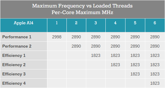
Of course, the old adage about having a very wide architecture is that you cannot clock it as high as something narrower. This is somewhat true; however, I will not draw any conclusions about Apple’s designs’ performance on higher power devices. On the new iPhone’s A14, the new Firestorm core can reach clock speeds of 3GHz, and when two cores are working simultaneously, the clock speed can drop to 2.89GHz.
We will detail power consumption later, but I currently see that Apple is limited by the actual thermal constraints of mobile devices rather than the inherent clock ceilings of the microarchitecture. The new Firestorm core’s clock speed is roughly on par with other mobile CPU microarchitectures on ARM, even though its design is broader. Therefore, the argument that designs must lower clock speeds due to increased complexity does not seem to apply in this instance. What Apple can do in high-temperature packaged devices like laptops, and in wall-mounted devices like Macs, will be very interesting.
Dominating Mobile Performance
Before we delve into the debate between x86 and Apple Silicon, it is necessary to take a closer look at how the A14 Firestorm core has improved over the A13 Lightning core, as well as a detailed introduction to the power and efficiency improvements of the new chip’s 5nm process node.
In this comparison, the process node is actually a wildcard, as the A14 is the first 5nm chip on the market, followed closely by Huawei’s Mate 40 series Kirin 9000. We happen to have devices and chips internally for testing, comparing the Kirin 9000 (Cortex-A77 at 3.13GHz on N5) and Snapdragon 865+ (Cortex-A77 at 3.09GHz on N7P), we can infer to some extent how much impact the process node has on power and efficiency, translating these improvements into a comparison between A13 and A14.
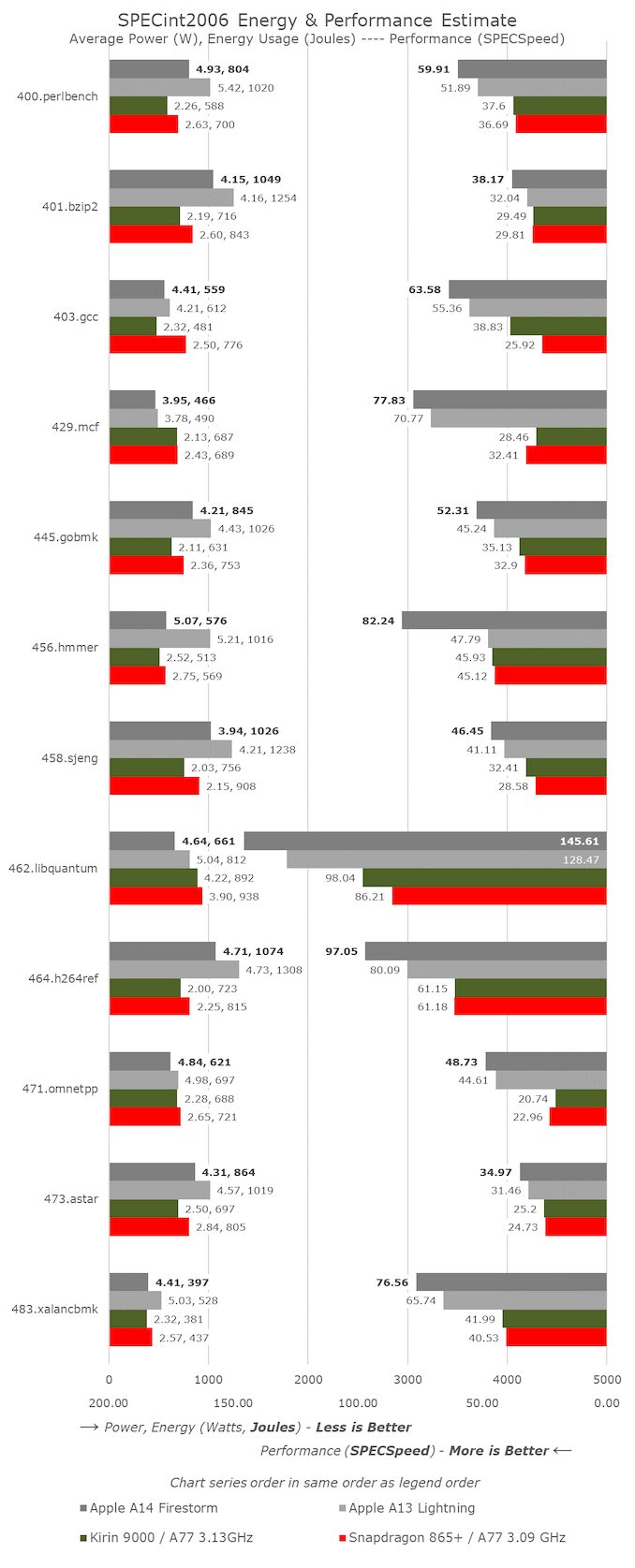
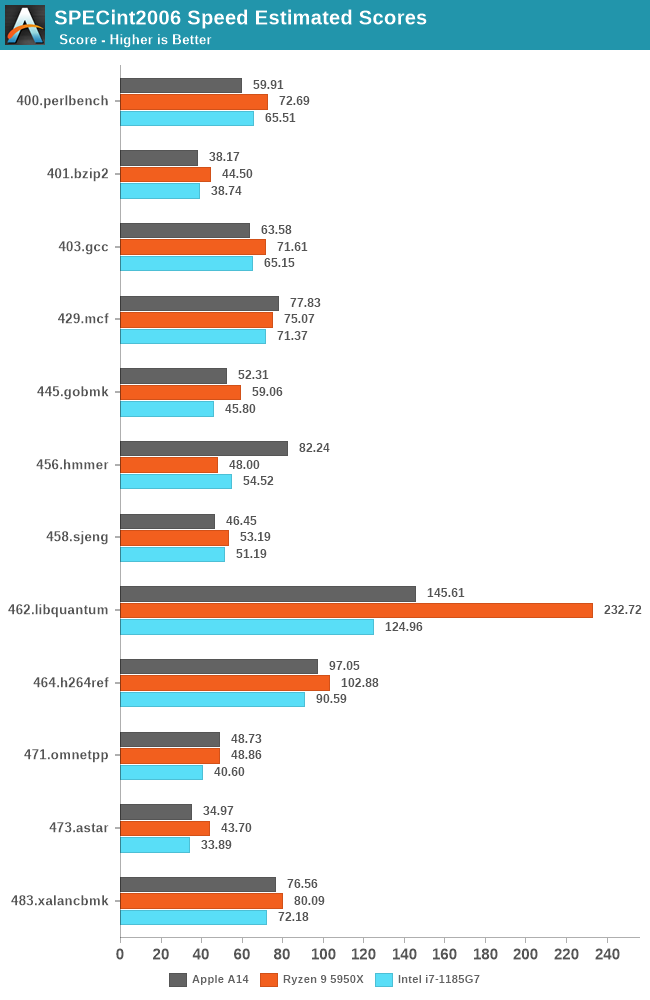
From SPECint2006, we have not seen anything unusual in A14’s scores, except for the massive improvement of 456. In fact, this is not due to a leap in microarchitecture, but rather new optimizations introduced in the new LLVM version in Xcode 12. Here, the compiler seems to have utilized loop optimizations similar to those found in GCC8. A13’s score actually increased from 47.79 to 64.87, but I have not run the new numbers across the entire suite yet.
For the rest of the workloads, A14 generally looks like a linear process relative to A13, as clock frequency increases from 2.66GHz to 3GHz. The overall IPC increase is around 5%, slightly lower than Apple’s previous generations, but the increase in clock speed is greater than usual.
The new chip’s power consumption is actually consistent, sometimes even better than A13, meaning this generation’s workload energy efficiency has seen significant improvements even at peak performance points.
Compared to contemporary Android and Cortex-core based SoCs, Apple’s performance seems quite unbalanced. The most prominent point is memory-intensive, sparse memory workloads (such as 429.mcf and 471.omnetpp), where Apple’s design capabilities far exceed performance by more than double, even though all chips are running similar mobile-level LPDDR4X/LPDDR5 memory. In our microarchitecture investigation, we found signs of “memory magic” in Apple’s designs, and we might speculate that they are using some sort of pointer-following prefetch mechanism.
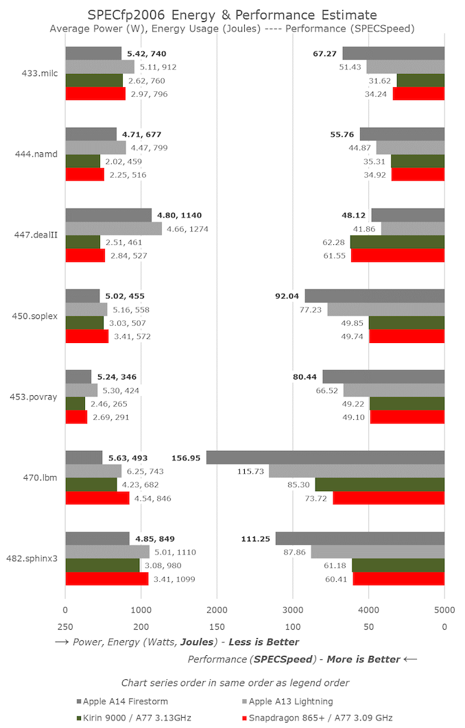
In SPECfp, the A14’s growth over the A13 is slightly higher than the linear clock frequency increase, as we measured a 10-11% IPC rise here. Given the additional fourth FP/SIMD pipeline in the design, this is not too surprising, while the integer portion of the core remains relatively unchanged compared to A13.
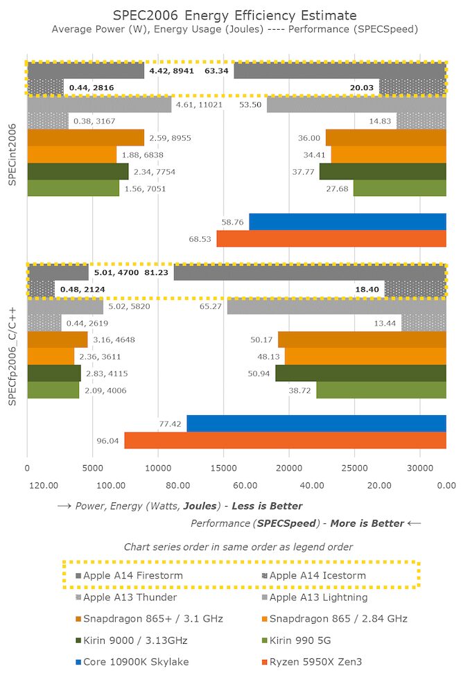
In overall mobile comparisons, we can see that the new A14 has achieved a strong improvement in performance over the A13. Compared to competitors, Apple is far ahead—we will have to wait until next year’s Cortex-X1 devices to see the gap narrow again.
Another very important point to note is that Apple has maintained a flat state while achieving all this, even reducing the power consumption of the new chip, significantly lowering energy consumption under the same workload.
Looking at the Kirin 9000 and Snapdragon 865+, we find that power drops by 10% for relatively similar performance. Both chips use the same CPU IP, just with different process nodes and implementations. It seems that Apple’s A14 is not only able to achieve process node improvements but also achieve better data, considering it is also a new microarchitecture design.
One more point to note is the data of the A14 small efficiency cores. In this generation, we have seen massive microarchitecture improvements in these new cores, with performance increased by 35% compared to last year’s A13 efficiency cores, while further reducing power consumption. I do not know how the small cores will play a role in Apple’s “Apple Silicon” Mac designs, but they are certainly still very efficient and effective compared to other current modern Arm designs.
Finally, there is the performance comparison between x86 and Apple. Typically for iPhone commentary, I would comment on this in this section of the article, but given the context today and the goals Apple has set for Apple Silicon, let’s dedicate a complete specialized chapter to this issue…
What Happens When Moving from Mobile Devices to Mac?
So far, our performance comparisons of Apple chipsets have been conducted in the context of iPhone reviews, with content comparing x86 designs being just a small footnote in this article. Today’s Apple Silicon launch completely changes our description of performance, putting aside the typical comparisons of apples to oranges that people usually argue about.
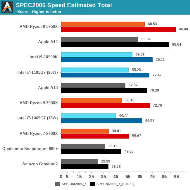
We currently do not have Apple Silicon devices, and it is likely we will not be using them for several weeks, but we do have the A14 and expect the new Mac chips to be based on the microarchitecture we see in iPhone designs. Of course, we are still comparing mobile chips with high-end laptop and even high-end desktop chips, but given the performance numbers, that is precisely the point we want to make here, which is the minimum standard that Apple’s newly launched Apple Silicon Mac chips can achieve.
The performance numbers for the A14 on this chart are incredible. If I published this data while hiding the A14 label, one might guess these data points come from AMD or Intel’s other x86 SKUs. The A14 can currently compete with the best top-tier performance designs that x86 vendors have on the market today, which is truly an impressive feat.
Looking at the detailed scores, I am again surprised that the A14 not only keeps up but generally performs much better than Intel’s CPU designs. If it weren’t for the recently released Zen3 designs, AMD wouldn’t look very good either.
Across the entire SPEC2006 chart, the A14 performs exceptionally well, leading in absolute performance over AMD’s recent Ryzen 5000 series.
In fact, Apple has achieved this in a device with total power consumption of 5W, including SoC, DRAM, and regulators, while devices without DRAM or regulators consume +21W (1185G7) and 49W (5950X). This is absolutely astonishing.
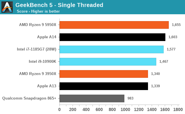
For more common benchmark suites like GeekBench, there have already been many criticisms, but frankly, I find these concerns or arguments to be completely unfounded. The only actual difference between the workloads in SPEC and those in GB5 is that the latter has fewer outlier tests, meaning it is more of a CPU benchmark while SPEC leans more towards CPU + DRAM.
Apple performs excellently in both workloads, which proves they have an extremely balanced microarchitecture, and Apple Silicon will be able to scale to “desktop workloads” in performance without too much issue.
Where Do Performance Trajectories Ultimately Intersect?
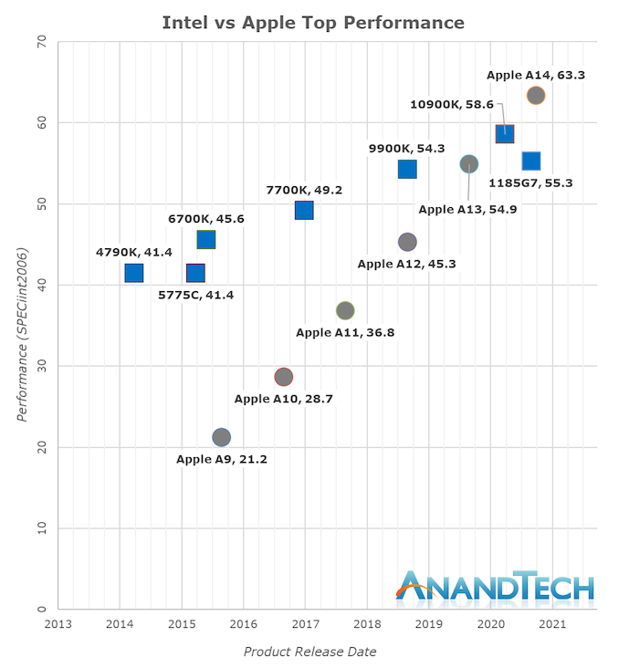
During the release of the A7, people scoffed at Apple’s claim that its microarchitecture was desktop-class. People were very dismissive of our performance data a few years ago when we called the A11 and A12 close to desktop levels, and today marks an important moment in the industry, as the Apple A14 can now clearly showcase the best performance that Intel can offer. This is a performance trajectory that has been steadily executed and progressed over the years:
In the past five years, Intel has successfully increased their best single-thread performance by about 28%, while Apple has successfully improved their designs by 198%, or 2.98 times the performance of Apple’s A9 at the end of 2015 (3 times).
These years of performance trajectory and undeniable execution capability have made Apple Silicon a reality today. Anyone who sees the absurdity of this chart will realize that Apple had no choice but to abandon Intel and x86 in favor of its own internal microarchitecture—staying put would mean stagnation and worse consumer products.
Today’s announcement only involves Apple notebook-level Apple Silicon chips, and while we do not know the details of what products Apple will launch as we write this, Apple’s massive energy efficiency advantage means the new chips will be able to deliver significantly extended battery life and/or greatly enhanced performance over the current Intel MacBook product line.
Apple claims they will completely transition their entire consumer product line to Apple Silicon chips within two years, which also suggests we will see the future Mac Pro adopting high TDP multi-core designs. If the company can continue its current performance trajectory, it will look very impressive.
Apple Aims for the Stars: Current x86 Should Be Careful
The previous few pages were written before Apple officially announced the new M1 chip. We have seen the impressive performance of the A14, which has surpassed the best performance that Intel can offer. The performance of the new M1 should be significantly higher than this level.
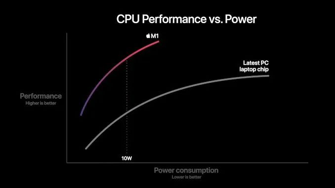
During the demonstration, we will review several slides from Apple to see what to expect in terms of performance and efficiency. In particular, the performance/power curve, which is the most detailed information Apple currently shares:
In this chart, Apple shows the new M1 chip, whose CPU power consumption peaks at around 18W. Competing PC notebook chips peak in the range of 35-40W, so this data is certainly not single-thread performance data but rather full-chip multi-thread performance. We do not know if this is comparing the M1 with AMD Renoir chips or Intel’s ICL or TGL chips, but in either case, the same general conclusion applies:
Apple has utilized a more advanced microarchitecture that provides significant IPC and achieves high performance at low core clocks, improving power efficiency significantly compared to existing x86 processors. The graph shows that the M1 offers about a 40% performance boost at peak, with only 40% of the power consumption compared to existing competing products.
Apple’s comparisons of random performance points are worthy of criticism, but the claim that its performance is 2.5 times that of the 10W measurement point is indeed reasonable, as this is based on the nominal TDP of the chip used in Intel’s MacBook Air. Likewise, this is due to the energy efficiency characteristics Apple has already achieved in the mobile space, so the M1 is expected to demonstrate such a significant gain—it certainly matches our A14 data.
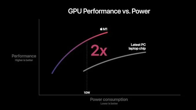
Today, we primarily discussed CPU issues, as this is where an unprecedented industry shift is taking place. However, we should not forget the GPU, as the new M1 represents Apple’s first custom design introduced into the Mac space.
Apple’s statements regarding performance and efficiency indeed lack context, as we do not know what their comparison points are. I will not attempt to build theories here, as there are too many variables at play, and we do not know enough details.
What we do know is that in the mobile space, Apple is absolutely leading in performance and efficiency. The last time we tested the A12Z, its design far exceeded integrated graphics designs. But since then, both AMD and Intel have made more significant leaps.
Apple claims the M1 is the world’s fastest CPU. Based on our data, the A14 has beaten all Intel designs, just falling short of AMD’s latest Zen3 chip—with higher clock speeds above 3GHz, larger L2 caches, and released TDP, we can certainly believe that Apple and the M1 can achieve this.
This moment has been brewing for years, and the new Apple Silicon is both shocking and highly anticipated. In the coming weeks, we will try to get our hands on the new hardware and confirm Apple’s claims.
Intel has stagnated in the market and lost a major customer today. AMD has made significant strides recently, but catching up to Apple’s power efficiency remains a considerable challenge. If Apple’s performance trajectory continues at this pace, the performance crown of x86 may never be regained.
★ Click the end of the article 【Read the original text】 to view the original link of this article.