Follow+Star Public Number, Don’t Miss Exciting Content
Author | strongerHuang
WeChat Official Account | Embedded Column
Bit-banding operations may not be used as much nowadays, but in the past when MCU performance was not very good, bit-banding was a common operation for many software engineers.
This article mainly discusses the Cortex-M3 core (STM32F1), which many friends may have found confusing when first learning.
1About Bit-Banding Operations
Bit-banding, abbreviated as bit-band, is also referred to as bit-segment. After supporting bit-banding operations, you can use ordinary load/store instructions to read and write individual bits.
Many friends who learned from the 51 microcontroller know that the P1.1 pin can be controlled individually; the pin we are operating on is a Bit.
We all know that in STM32, you cannot directly operate on a specific Bit of a register, for example, to control the output of data register ODR1 on the PA port individually, as shown in the figure below:
The STM32F1 core Cortex-M3 has long considered this issue, to achieve direct operation on Bit positions like ODR1, it has opened up a block of address space (strong>bit-band alias) in the core: you can map Bit positions like ODR1 (strong>bit-band region) to the corresponding address in the bit-band alias area. You only need to operate on the mapped address to manipulate the ODR1 bit.
In simple terms, it is a mapping operation, but this mapping operation has many conventions to follow.
2Mapping Relationships in Bit-Banding Operations
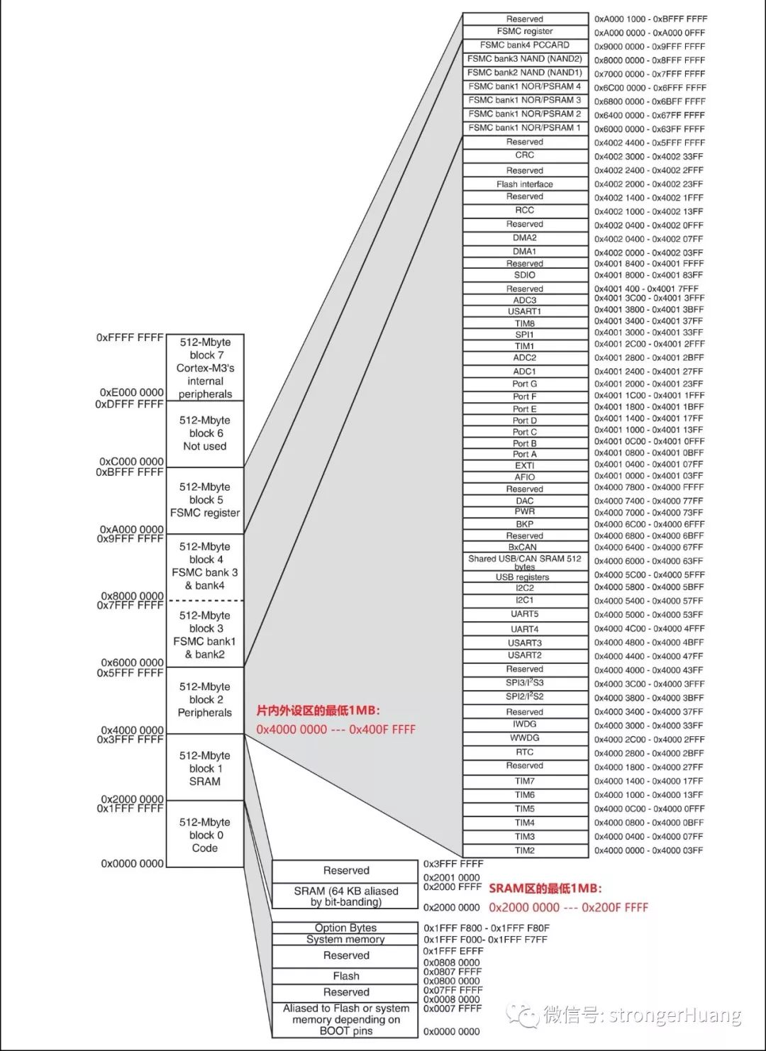
In Cortex-M3, there are two areas that implement bit-banding operations, one is the SRAM area with the lowest 1MB range, and the second is the on-chip peripheral area with the lowest 1MB range.
These two areas are highlighted in red in the figure below:
These two 1MB will be mapped to two other address areas:
1. The lowest 1MB of the SRAM area (0x2000 0000 — 0x200F FFFF) maps to (0x2200 0000 — 0x23FF FFFF).
2. The lowest 1MB of the on-chip peripheral area (0x4000 0000 — 0x400F FFFF) maps to (0x4200 0000 — 0x43FF FFFF).
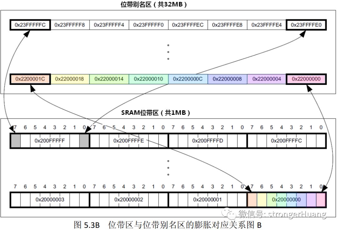
In fact, it is mapped to an offset (distance from itself) of 0x0200 0000 outside the 32MB space (bit-band alias area), as shown in the mapping relationship of SRAM area:
Tip: The colored 8Bit in the figure is mapped to an offset 0x0200 0000 outside the 32Bit (4Byte) space. When we read and write to address 0x2200 0000, we are actually manipulating Bit0 in 0x2000 0000.
This is the so-called “bit expansion correspondence“, where 1Bit expands to 32Bit (4 bytes). The 4 bytes correspond to the address of that 1Bit, and the data in that address is only valid for the least significant bit (LSB)..
Explanation of keywords that appear multiple times above:
Bit-band region: The address region that supports bit-banding operations;
Bit-band alias: Access to the alias address ultimately acts on the access to the bit-band region;
3Bit-band Region -> Alias Region Calculation Formula
The main purpose of bit-banding operations: to calculate the alias region address (AliasAddr) from the bit address (A).
1. SRAM Area Calculation Formula
AliasAddr = 0x22000000 + ((A−0x20000000)*8+n)*4 = 0x22000000+(A-0x20000000)*32 + n*4
2. On-chip Peripheral Area Calculation Formula
AliasAddr = 0x42000000 + ((A-0x40000000)*8+n)*4 = 0x42000000+(A-0x40000000)*32 + n*4
Since the mapping relationship is the same, the principle of the formula is also the same, only the addresses are different. The calculation formula needs to be understood in conjunction with the above figure bit expansion correspondence.
*8: 1 word is 4 bytes;
*4: 1 byte is 8 bits;
Using the above calculation formula, the process of code implementation is very simple; our goal is to perform read/write operations on the “AliasAddr” address.
1. RAM Bit-Banding Macro Definition
#define BITBAND_RAM(RAM, BIT) (*((uint32_t volatile*)(0x22000000u + (((uint32_t)&(RAM) - (uint32_t)0x20000000u)<<5) + (((uint32_t)(BIT))<<2))))
2. Peripheral Register Bit-Banding Macro Definition
#define BITBAND_REG(REG, BIT) (*((uint32_t volatile*)(0x42000000u + (((uint32_t)&(REG) - (uint32_t)0x40000000u)<<5) + (((uint32_t)(BIT))<<2))))
To facilitate comparison, here is a screenshot:

A. Write 0 to Bit1 of RAM address 0x20001000
BITBAND_RAM(*(uint32_t *)0x20001000, 1) = 0;
B. Read Bit1 of RAM address 0x20001000
uint8_t Val;Val=BITBAND_RAM(*(uint32_t *)0x20001000, 1);
C. Output 1 to the data output register of PA1
BITBAND_REG(GPIOA->ODR, 1) = 1;
D. Read the data output register of PA1
uint8_t Val;Val=BITBAND_REG(GPIOA->ODR, 1);
This is to operate on a specific address, similar to operating on a pointer;
5Advantages and Disadvantages of Bit-Banding Operations
1. Advantages
Compared to directly operating on registers, the code is more concise, and the execution efficiency is higher. It avoids confusion in multi-tasking or interrupt situations.
2. Disadvantages
Improper operation (incorrect address parameter) can easily lead to bus faults.
For more details on bit-banding operations in Cortex-M3, please refer to the Cortex-M3 Technical Reference Manual (Authoritative Guide).
The later Cortex-M processors no longer support bit-banding operations, so from the perspective of compatibility with future software, it is not highly recommended to continue using it.
However, bit-banding operations are a classic, and I share this for everyone to understand, hoping it will be helpful to you.
Reply in the background 『Cortex-M』『STM32』 to read more related articles.
Follow the WeChat official account 『Embedded Column』 for more content at the bottom menu, reply “Join Group” to join the technical exchange group as per the rules.

Click “Read Original” to see more shares. Welcome to share, collect, like, and view.


